Datasheet 搜索 > 逻辑芯片 > TI(德州仪器) > SN74LVC2G04DBVR 数据手册 > SN74LVC2G04DBVR 产品手册 1/13 页

¥ 0.407
SN74LVC2G04DBVR 产品手册 - TI(德州仪器)
制造商:
TI(德州仪器)
分类:
逻辑芯片
封装:
SOT-23-6
描述:
TEXAS INSTRUMENTS SN74LVC2G04DBVR. 芯片, 双路非门, SOT-23-6, 整卷
Pictures:
3D模型
符号图
焊盘图
引脚图
产品图
页面导航:
导航目录
SN74LVC2G04DBVR数据手册
Page:
of 13 Go
若手册格式错乱,请下载阅览PDF原文件
www.ti.com
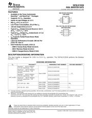
FEATURES
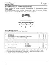
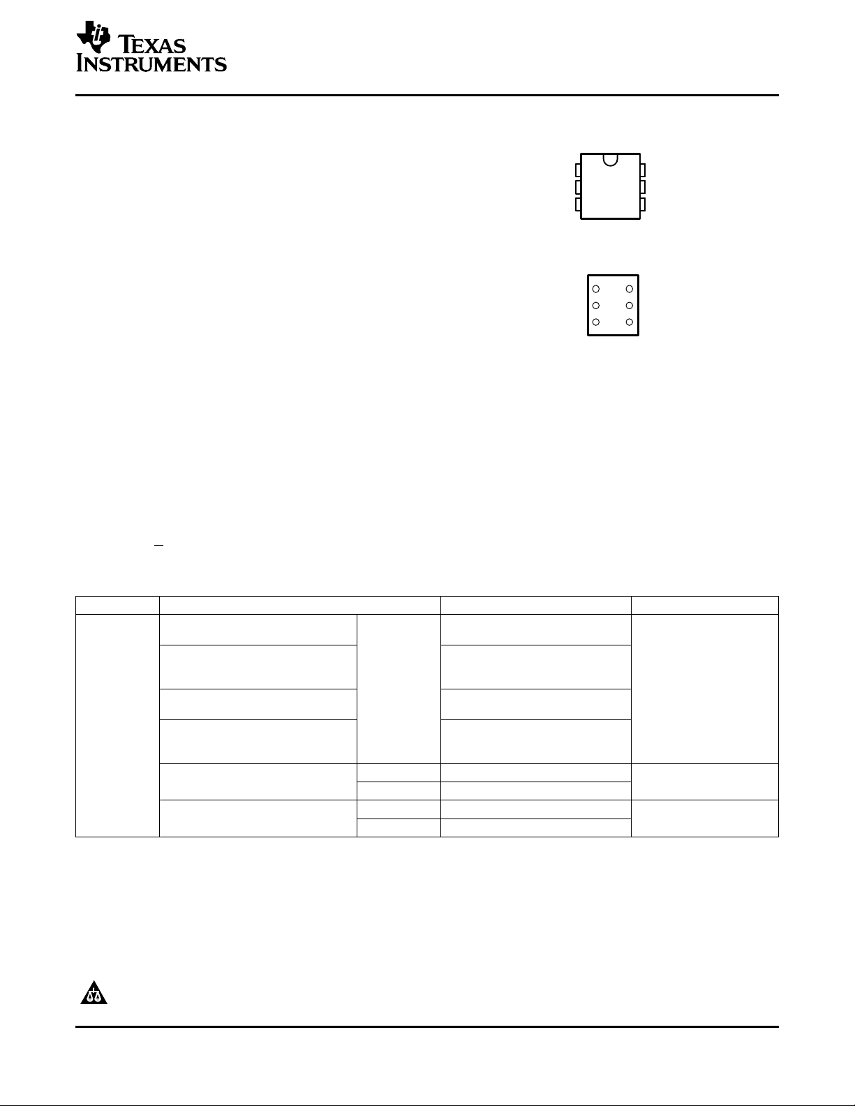
DBV OR DCK PACKAGE
(TOP VIEW)
1
2
3
6
5
4
1A
GND
2A
1Y
V
CC
2Y
3
2
1
4
5
6
2A
GND
1A
2Y
V
CC
1Y
YEA, YEP, YZA, OR YZP PACKAGE
(BOTTOM VIEW)
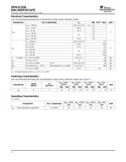
DESCRIPTION/ORDERING INFORMATION
SN74LVC2G04
DUAL INVERTER GATE
SCES195J – APRIL 1999 – REVISED JULY 2005
• Available in the Texas Instruments
NanoStar™ and NanoFree™ Packages
• Supports 5-V V
CC
Operation
• Inputs Accept Voltages to 5.5 V
• Max t
pd
of 4.1 ns at 3.3 V
• Low Power Consumption, 10- µ A Max I
CC
• ± 24-mA Output Drive at 3.3 V
• Typical V
OLP
(Output Ground Bounce) <0.8 V
at V
CC
= 3.3 V, T
A
= 25 ° C
• Typical V
OHV
(Output V
OH
Undershoot) >2 V at
V
CC
= 3.3 V, T
A
= 25 ° C
• I
off
Supports Partial-Power-Down Mode
Operation
• Latch-Up Performance Exceeds 100 mA Per
JESD 78, Class II
• ESD Protection Exceeds JESD 22
– 2000-V Human-Body Model (A114-A)
– 200-V Machine Model (A115-A)
– 1000-V Charged-Device Model (C101)
This dual inverter is designed for 1.65-V to 5.5-V V
CC
operation. The SN74LVC2G04 performs the Boolean
function Y = A.
ORDERING INFORMATION
T
A
PACKAGE
(1)
ORDERABLE PART NUMBER TOP-SIDE MARKING
(2)
NanoStar™ – WCSP (DSBGA)
SN74LVC2G04YEAR
0.17-mm Small Bump – YEA
NanoFree™ – WCSP (DSBGA)
0.17-mm Small Bump – YZA SN74LVC2G04YZAR
(Pb-free)
Reel of 3000 _ _ _CC_
NanoStar™ – WCSP (DSBGA)
SN74LVC2G04YEPR
0.23-mm Large Bump – YEP
–40 ° C to 85 ° C
NanoFree™ – WCSP (DSBGA)
0.23-mm Large Bump – YZP SN74LVC2G04YZPR
(Pb-free)
Reel of 3000 SN74LVC2G04DBVR
SOT (SOT-23) – DBV C04_
Reel of 250 SN74LVC2G04DBVT
Reel of 3000 SN74LVC2G04DCKR
SOT (SC-70) – DCK CC_
Reel of 250 SN74LVC2G04DCKT
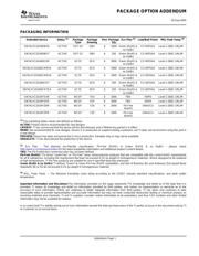
(1) Package drawings, standard packing quantities, thermal data, symbolization, and PCB design guidelines are available at
www.ti.com/sc/package.
(2) DBV/DCK: The actual top-side marking has one additional character that designates the assembly/test site.
YEA/YZA,YEP/YZP: The actual top-side marking has three preceding characters to denote year, month, and sequence code, and one
following character to designate the assembly/test site. Pin 1 identifier indicates solder-bump composition (1 = SnPb, • = Pb-free).
Please be aware that an important notice concerning availability, standard warranty, and use in critical applications of Texas
Instruments semiconductor products and disclaimers thereto appears at the end of this data sheet.
NanoStar, NanoFree are trademarks of Texas Instruments.
PRODUCTION DATA information is current as of publication date.
Copyright © 1999–2005, Texas Instruments Incorporated
Products conform to specifications per the terms of the Texas
Instruments standard warranty. Production processing does not
necessarily include testing of all parameters.
器件 Datasheet 文档搜索
AiEMA 数据库涵盖高达 72,405,303 个元件的数据手册,每天更新 5,000 多个 PDF 文件
