Datasheet 搜索 > 电压基准芯片 > ADI(亚德诺) > AD584KH 数据手册 > AD584KH 产品设计参考手册 1/13 页

¥ 0.073
AD584KH 产品设计参考手册 - ADI(亚德诺)
制造商:
ADI(亚德诺)
分类:
电压基准芯片
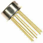
封装:
TO-99-8
描述:
引脚可编程精密基准电压源 Pin Programmable Precision Voltage Reference
Pictures:
3D模型
符号图
焊盘图
引脚图
产品图
页面导航:
导航目录
AD584KH数据手册
Page:
of 13 Go
若手册格式错乱,请下载阅览PDF原文件
Pin Programmable,
Precision Voltage Reference
Data Sheet
AD584
Rev. C
Information furnished by Analog Devices is believed to be accurate and reliable. However, no
responsibility is assumed by Analog Devices for its use, nor for any infringements of patents or other
rights of third parties that may result from its use. Specifications subject to change without notice. No
license is granted by implication or otherwise under any patent or patent rights of Analog Devices.
Trademarks and registered trademarks are the property of their respective owners.
One Technology Way, P.O. Box 9106, Norwood, MA 02062-9106, U.S.A.
Tel: 781.329.4700
www.analog.com
Fax: 781.461.3113 ©1978–2012 Analog Devices, Inc. All rights reserved.
FEATURES
Four programmable output voltages
10.000 V, 7.500 V, 5.000 V, and 2.500 V
Laser-trimmed to high accuracies
No external components required
Trimmed temperature coefficient
15 ppm/°C maximum, 0°C to 70°C (AD584K)
15 ppm/°C maximum, −55°C to +125°C (AD584T)
Zero output strobe terminal provided
2-terminal negative reference: capability (5 V and above)
Output sources or sinks current
Low quiescent current: 1.0 mA maximum
10 mA current output capability
MIL-STD-883 compliant versions available
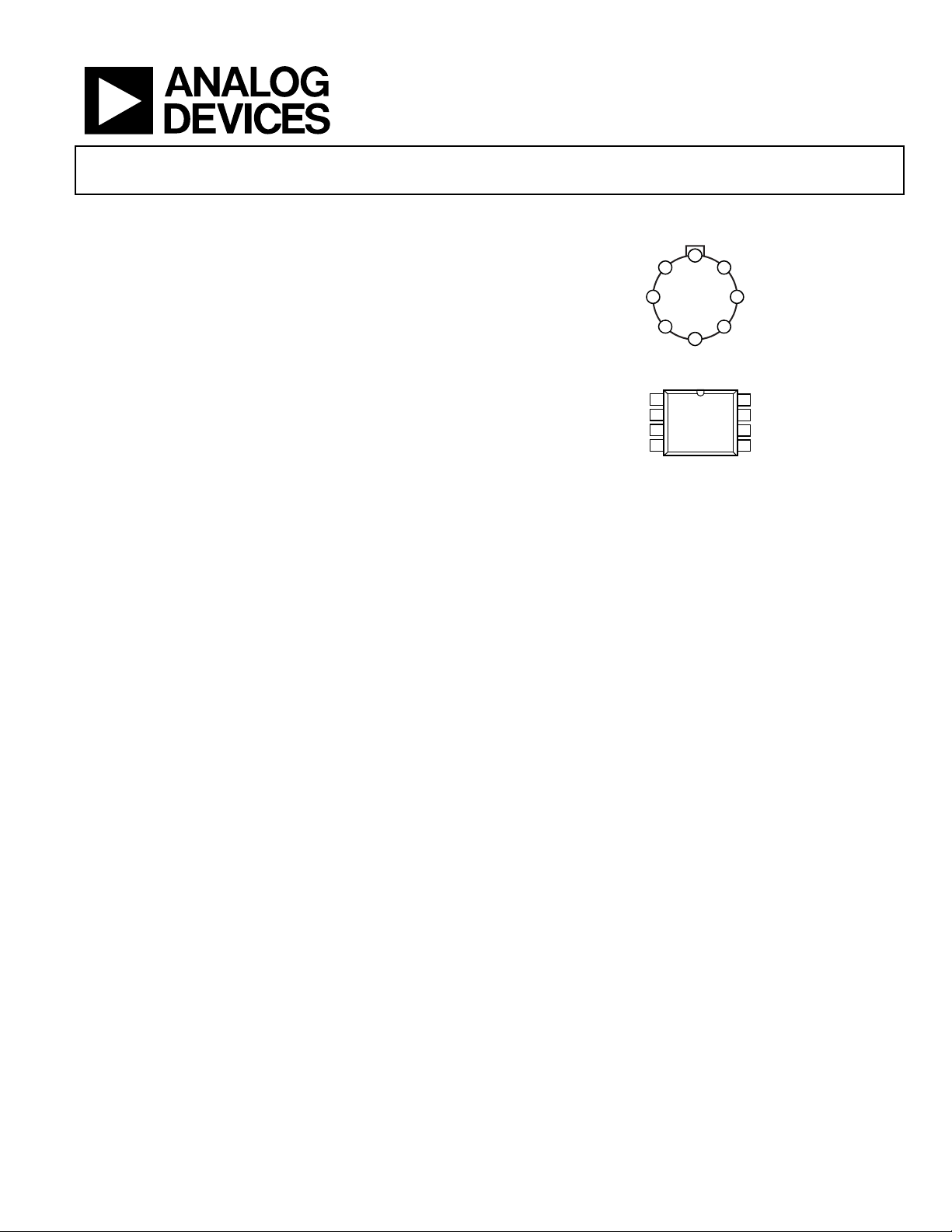
PIN CONFIGURATIONS
Figure 1. 8-Pin TO-99
Figure 2. 8-Lead PDIP
GENERAL DESCRIPTION
The AD584 is an 8-terminal precision voltage reference offering
pin programmable selection of four popular output voltages:
10.000 V, 7.500 V, 5.000 V and 2.500 V. Other output voltages,
above, below, or between the four standard outputs, are available by
the addition of external resistors. The input voltage can vary
between 4.5 V and 30 V.
Laser wafer trimming (LWT) is used to adjust the pin
programmable output levels and temperature coefficients,
resulting in the most flexible high precision voltage reference
available in monolithic form.
In addition to the programmable output voltages, the AD584
offers a unique strobe terminal that permits the device to be
turned on or off. When the AD584 is used as a power supply
reference, the supply can be switched off with a single, low power
signal. In the off state, the current drained by the AD584 is reduced
to approximately 100 µA. In the on state, the total supply current is
typically 750 µA, including the output buffer amplifier.
The AD584 is recommended for use as a reference for 8-, 10-,
or 12-bit digital-to-analog converters (DACs) that require an
external precision reference. In addition, the device is ideal for
analog-to-digital converters (ADCs) of up to 14-bit accuracy,
either successive approximation or integrating designs, and in
general, it can offer better performance than that provided by
standard self-contained references.
The AD584J and AD584K are specified for operation from 0°C
to +70°C, and the AD584S and AD584T are specified for the
−55°C to +125°C range. All grades are packaged in a hermetically
sealed, eight-terminal TO-99 metal can, and the AD584J and
AD584K are also available in an 8-lead PDI P.
PRODUCT HIGHLIGHTS
1. The flexibility of the AD584 eliminates the need to design-
in and inventory several different voltage references.
Furthermore, one AD584 can serve as several references
simultaneously when buffered properly.
2. Laser trimming of both initial accuracy and temperature
coefficient results in very low errors overtemperature
without the use of external components.
3. The AD584 can be operated in a 2-terminal Zener mode at
a 5 V output and above. By connecting the input and the
output, the AD584 can be used in this Zener configuration
as a negative reference.
4. The output of the AD584 is configured to sink or source
currents. This means that small reverse currents can be
tolerated in circuits using the AD584 without damage to
the reference and without disturbing the output voltage
(10 V, 7.5 V, and 5 V outputs).
5. The AD584 is available in versions compliant with MIL-STD-
883. Refer to the Analog Devices current AD584/883B data
sheet for detailed specifications. This can be found under the
Additional Data Sheets section of the AD584 product page.
1
2 6
7
3 5
8
V+
TAB
4
AD584
TOP VIEW
(Not to Scale)
COMMON
STROBE
V
BG
CAP
2.5V
5.0V
10.0V
00527-001
10.0V
1
5.0V
2
2.5V
3
COMMON
4
V+
8
CAP
7
V
BG
6
STROBE
5
AD584
TOP VIEW
(Not to Scale)
00527-002
器件 Datasheet 文档搜索
AiEMA 数据库涵盖高达 72,405,303 个元件的数据手册,每天更新 5,000 多个 PDF 文件
