Datasheet 搜索 > 电压基准芯片 > ADI(亚德诺) > AD584KH 数据手册 > AD584KH 产品设计参考手册 6/13 页

¥ 0.073
AD584KH 产品设计参考手册 - ADI(亚德诺)
制造商:
ADI(亚德诺)
分类:
电压基准芯片
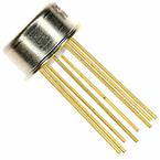
封装:
TO-99-8
描述:
引脚可编程精密基准电压源 Pin Programmable Precision Voltage Reference
Pictures:
3D模型
符号图
焊盘图
引脚图
产品图
页面导航:
导航目录
AD584KH数据手册
Page:
of 13 Go
若手册格式错乱,请下载阅览PDF原文件
AD584 Data Sheet
Rev. C | Page 6 of 12
THEORY OF OPERATION
APPLYING THE AD584
With power applied to Pin 8 and Pin 4 and all other pins open,
the AD584 produces a buffered nominal 10.0 V output between
Pin 1 and Pin 4 (see Figure 3). The stabilized output voltage can
be reduced to 7.5 V, 5.0 V, or 2.5 V by connecting the programming
pins as shown in Table 4.
Table 4.
Output
Voltage (V) Pin Programming
7.5 Join the 2.5 V (Pin 3) and 5.0 V (Pin 2) pins.
5.0 Connect the 5.0 V pin (Pin 2) to the output pin (Pin 1).
2.5 Connect the 2.5 V pin (Pin 3) to the output pin (Pin 1).
The options shown in Table 4 are available without the use of any
additional components. Multiple outputs using only one AD584
can be provided by buffering each voltage programming pin
with a unity-gain, noninverting op amp.
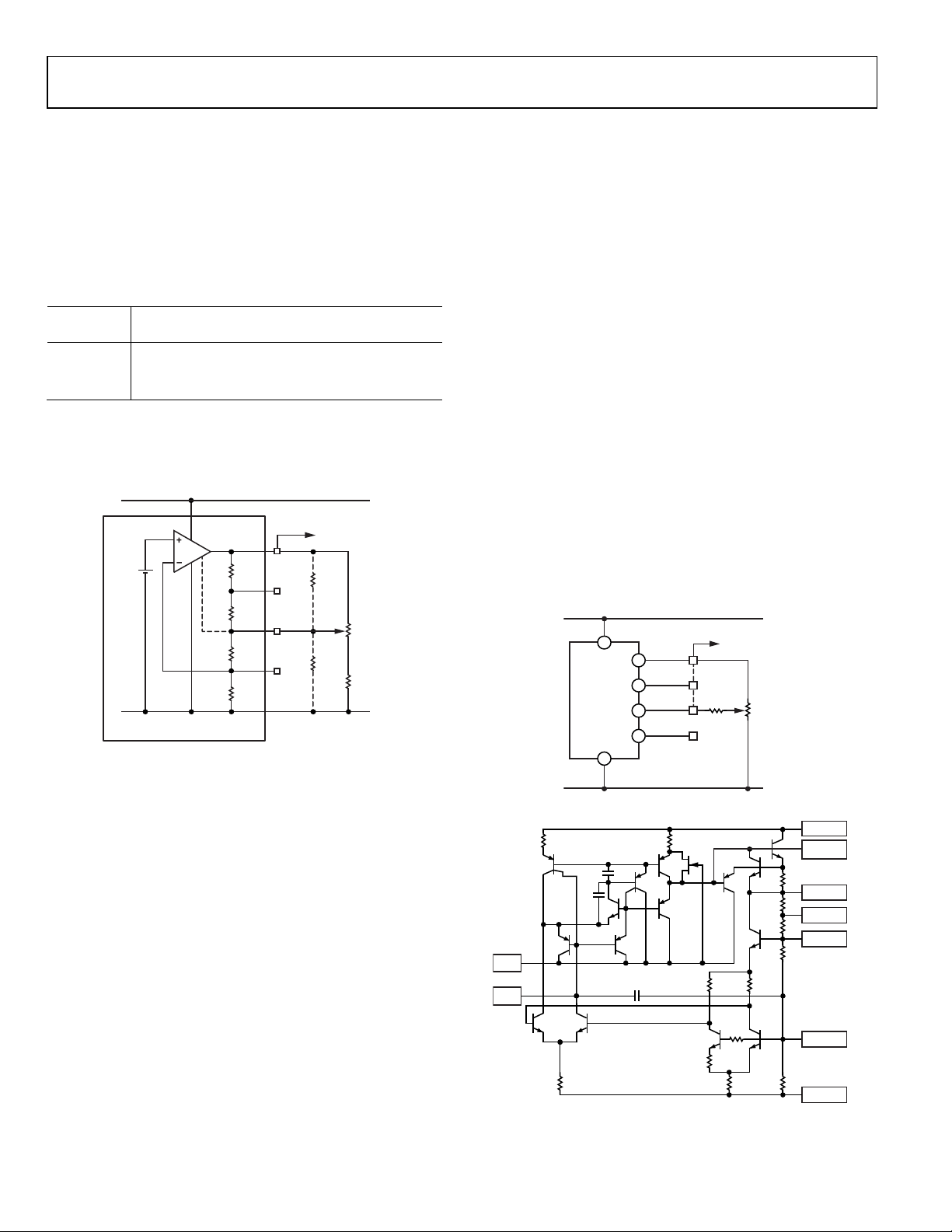
Figure 3. Variable Output Options
The AD584 can also be programmed over a wide range of output
voltages, including voltages greater than 10 V, by the addition
of one or more external resistors. Figure 3 illustrates the general
adjustment procedure, with approximate values given for the
internal resistors of the AD584. The AD584 may be modeled
as an op amp with a noninverting feedback connection, driven
by a high stability 1.215 V band gap reference (see Figure 5 for
schematic).
When the feedback ratio is adjusted with external resistors, the
output amplifier can be made to multiply the reference voltage
by almost any convenient amount, making popular outputs of
10.24 V, 5.12 V, 2.56 V, or 6.3 V easy to obtain. The most general
adjustment (which gives the greatest range and poorest resolution)
uses R1 and R2 alone (see Figure 3). As R1 is adjusted to its upper
limit, the 2.5V pin (Pin 3) is connected to the output, which
reduces to 2.5 V. As R1 is adjusted to its lower limit, the output
voltage rises to a value limited by R2. For example, if R2 is
approximately 6 kΩ, the upper limit of the output range is
approximately 20 V, even for the large values of R1. Do not
omit R2; choose its value to limit the output to a value that can
be tolerated by the load circuits. If R2 is zero, adjusting R1 to its
lower limit results in a loss of control over the output voltage.
When precision voltages are set at levels other than the standard
outputs, account for the 20% absolute tolerance in the internal
resistor ladder.
Alternatively, the output voltage can be raised by loading the
2.5 V tap with R3 alone. The output voltage can be lowered by
connecting R4 alone. Either of these resistors can be a fixed
resistor selected by test or an adjustable resistor. In all cases, the
resistors should have a low temperature coefficient to match the
AD584 internal resistors, which have a negative temperature
coefficient less than 60 ppm/°C. If both R3 and R4 are used,
these resistors should have matching temperature coefficients.
When only small adjustments or trims are required, the circuit
in Figure 4 offers better resolution over a limited trim range. The
circuit can be programmed to 5.0 V, 7.5 V, or 10 V, and it can be
adjusted by means of R1 over a range of about ±200 m V. To trim
the 2.5 V output option, R2 (see Figure 4) can be reconnected to
the band gap reference (Pin 6). In this configuration, limit the
adjustment to ±100 mV to avoid affecting the performance of
the AD584.
Figure 4. Output Trimming
Figure 5. Schematic Diagram
AD584
V
SUPPLY
V
OUT
8
1
2
3
6
1.215V
10V
5V
*
2.5V
12kΩ
6kΩ
V
BG
R4
4COMMON
R1
R2
R3
6kΩ
24kΩ
*THE 2.5V TAP IS USED INTERNALLY AS A BIAS POINT
AND SHOULD NOT BE CHANGED BY MORE THAN 100mV
IN ANY TRIM CONFIGURATION.
00527-004
AD584
V
OUT
1
10.0V
8
V+
4
COMMON
2
5.0V
3
2.5V
6
V
BG
R1
10kΩ
R2
300kΩ
00527-005
R38
R40
Q10
Q16
Q13
Q11
Q14
Q12
Q15
SUB
CAP
R41
R42
R34
R37
R35
R30
R31 R36
Q6
Q8
Q5
C51
C52
C50
Q20
Q7
STROBE
V+
OUT 10V
5V TAP
2.5V TAP
V
BG
V–
R32R33
Q3 Q4
Q2
Q1
R39
00527-006
器件 Datasheet 文档搜索
AiEMA 数据库涵盖高达 72,405,303 个元件的数据手册,每天更新 5,000 多个 PDF 文件
