Datasheet 搜索 > ON Semiconductor(安森美) > AX8052F143-3-TX40 数据手册 > AX8052F143-3-TX40 产品设计参考手册 4/75 页

 器件3D模型
¥ 27.813
AX8052F143-3-TX40 产品设计参考手册 - ON Semiconductor(安森美)
制造商:
ON Semiconductor(安森美)
封装:
QFN-40
描述:
微控制器, 特定应用, AX80系列, AX8052F143系列, 8位, 64KB, 20MHz, QFN-40
Pictures:
3D模型
符号图
焊盘图
引脚图
产品图
页面导航:
导航目录
AX8052F143-3-TX40数据手册
Page:
of 75 Go
若手册格式错乱,请下载阅览PDF原文件
AND9347/D
www.onsemi.com
4
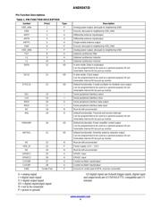
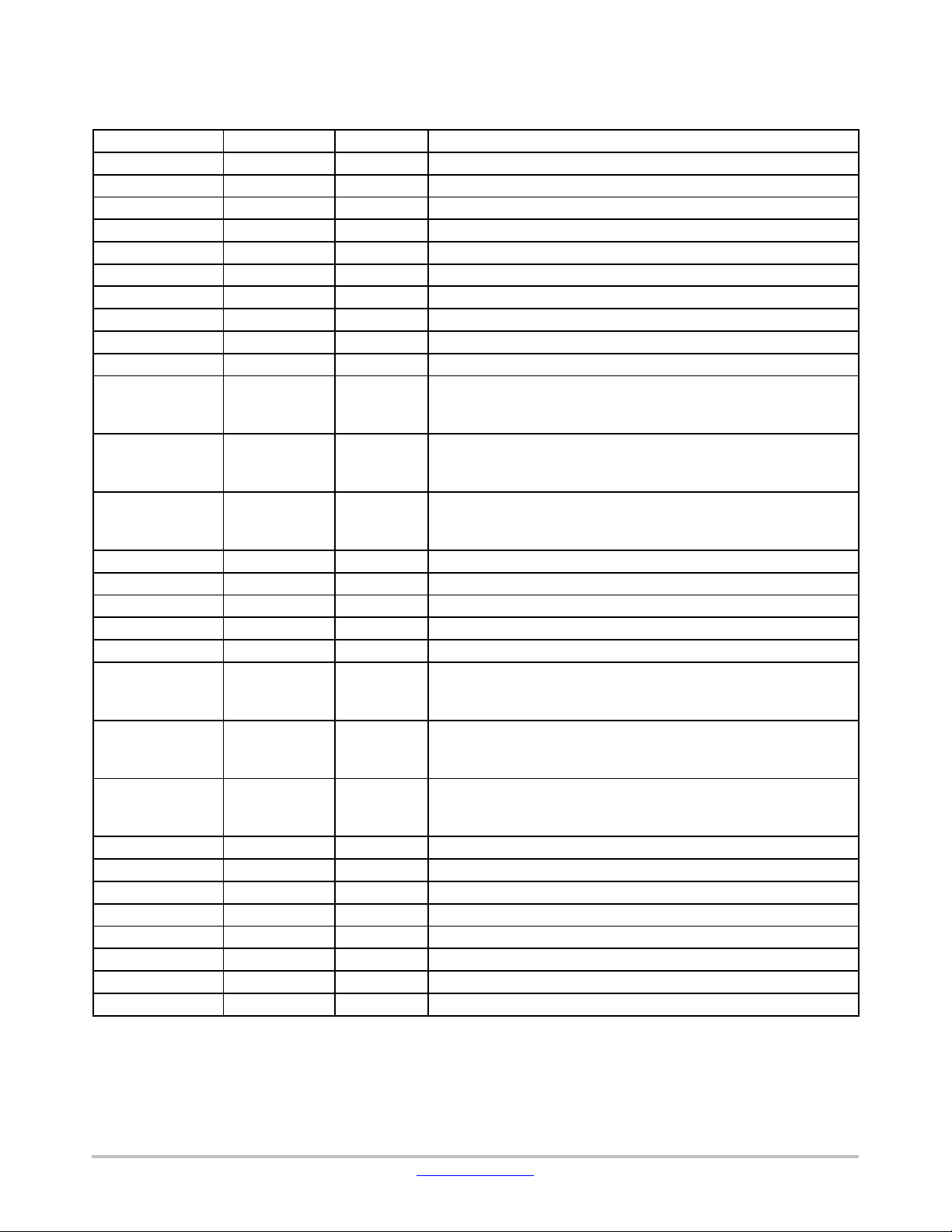
Pin Function Descriptions
Table 1. PIN FUNCTION DESCRIPTION
Symbol Pin(s) Type Description
VDD_ANA 1 P Analog power output, decouple to neighboring GND
GND 2 P Ground, decouple to neighboring VDD_ANA
ANTP 3 A Differential antenna input/output
ANTN 4 A Differential antenna input/output
ANTP1 5 A Single-ended antenna output
GND 6 P Ground, decouple to neighboring VDD_ANA
VDD_ANA 7 P Analog power output, decouple to neighboring GND
FILT 8 A Optional synthesizer filter
L2 9 A Optional synthesizer inductor
L1 10 A Optional synthesizer inductor
DATA 11 I/O In wire mode: Data in-out/output
Can be programmed to be used as a general purpose I/O pin
Selectable internal 65 kΩ pull-up resistor
DCLK 12 I/O In wire mode: Clock output
Can be programmed to be used as a general purpose I/O pin
Selectable internal 65 kΩ pull-up resistor
SYSCLK 13 I/O Default functionality: Crystal oscillator (or divided) clock output
Can be programmed to be used as a general purpose I/O pin
Selectable internal 65 kΩ pull-up resistor
SEL 14 I Serial peripheral interface select
CLK 15 I Serial peripheral interface clock
MISO 16 O Serial peripheral interface data output
MOSI 17 I Serial peripheral interface data input
NC 18 N Must be left unconnected
IRQ 19 O Default functionality: Transmit and receive interrupt
Can be programmed to be used as a general purpose I/O pin
Selectable internal 65 kΩ pull-up resistor
PWRAMP 20 I/O Default functionality: Power amplifier control output
Can be programmed to be used as a general purpose I/O pin
Selectable internal 65 kΩ pull-up resistor
ANTSEL 21 I/O Default functionality: Diversity antenna selection output
Can be programmed to be used as a general purpose I/O pin
Selectable internal 65 kΩ pull-up resistor
NC 22 N Must be left unconnected
VDD_IO 23 P Power supply 1.8 V – 3.6 V
NC 24 N Must be left unconnected
GPADC1 25 A GPADC input
GPADC2 26 A GPADC input
CLK16N 27 A Crystal oscillator input/output
CLK16P 28 A Crystal oscillator input/output
GND Center Pad P Ground on center pad of QFN, must be connected
A = analog signal
I = digital input signal
O = digital output signal
I/O = digital input/output signal
N = not to be connected
P = power or ground
All digital inputs are Schmitt trigger inputs, digital input
and output levels are LVCMOS/LVTTL compatible and 5 V
tolerant.
器件 Datasheet 文档搜索
AiEMA 数据库涵盖高达 72,405,303 个元件的数据手册,每天更新 5,000 多个 PDF 文件
