Datasheet 搜索 > ADI(亚德诺) > LT1027CCS8-5#PBF 数据手册 > LT1027CCS8-5#PBF 产品设计参考手册 3/8 页

¥ 61.099
LT1027CCS8-5#PBF 产品设计参考手册 - ADI(亚德诺)
制造商:
ADI(亚德诺)
封装:
05-08-1610 (S8)
描述:
串联 15mA
Pictures:
3D模型
符号图
焊盘图
引脚图
产品图
页面导航:
典型应用电路图在P6
技术参数、封装参数在P3
应用领域在P6
导航目录
LT1027CCS8-5#PBF数据手册
Page:
of 8 Go
若手册格式错乱,请下载阅览PDF原文件
LT1027
3
sn1027 1027fcs
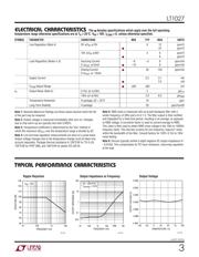
SYMBOL PARAMETER CONDITIONS MIN TYP MAX UNITS
Line Regulation (Note 4) 8V ≤ V
IN
≤ 10V 6 12 ppm/V
● 25 ppm/V
10V ≤ V
IN
≤ 40V 3 6 ppm/V
● 8 ppm/V
Load Regulation (Notes 4, 6) Sourcing Current –8 –3 6 ppm/mA
0 ≤ I
OUT
≤ 15mA ● –10 8 ppm/mA
Sinking Current ● 30 120 ppm/mA
0 ≥ I
OUT
≥ –10mA
Supply Current 2.2 3.1 mA
● 3.5 mA
V
TRIM
Adjust Range ● ±30 ±50 mV
e
n
Output Noise (Note 5) 0.1Hz ≤ f ≤ 10Hz 3 µV
P-P
10Hz ≤ f ≤ 1kHz 2.0 6.0 µV
RMS
Temperature Hysteresis H package; ∆T = 25°C 10 ppm
Long Term Stability H package 20 ppm/month
Note 5: RMS noise is measured with an 8-pole bandpass filter with a
center frequency of 30Hz and a Q of 1.5. The filter output is then rectified
and integrated for a fixed time period, resulting in an average, as opposed
to RMS voltage. A correction factor is used to convert average to RMS.
This value is then used to obtain RMS noise voltage in the 10Hz to 1000Hz
frequency band. This test also screens for low frequency "popcorn" noise
within the bandwidth of the filter. Consult factory for 100% 0.1Hz to 10Hz
noise testing.
Note 6: Devices typically exhibit a slight negative DC output impedance of
–0.015Ω. This compensates for PC trace resistance, improving regulation
at the load.
Note 1: Absolute Maximum Ratings are those values beyond which the life
of the part may be impaired.
Note 2: Output voltage is measured immediately after turn-on. Changes
due to chip warm-up are typically less than 0.005%.
Note 3: Temperature coefficient is determined by the "box" method in
which the maximum ∆V
OUT
over the temperature range is divided by ∆T.
Note 4: Line and load regulation measurements are done on a pulse basis.
Output voltage changes due to die temperature change must be taken into
account separately. Package thermal resistance is 150°C/W for TO-5 (H),
130°C/W for PDIP (N8), and 180°C/W for plastic SO (SO-8).
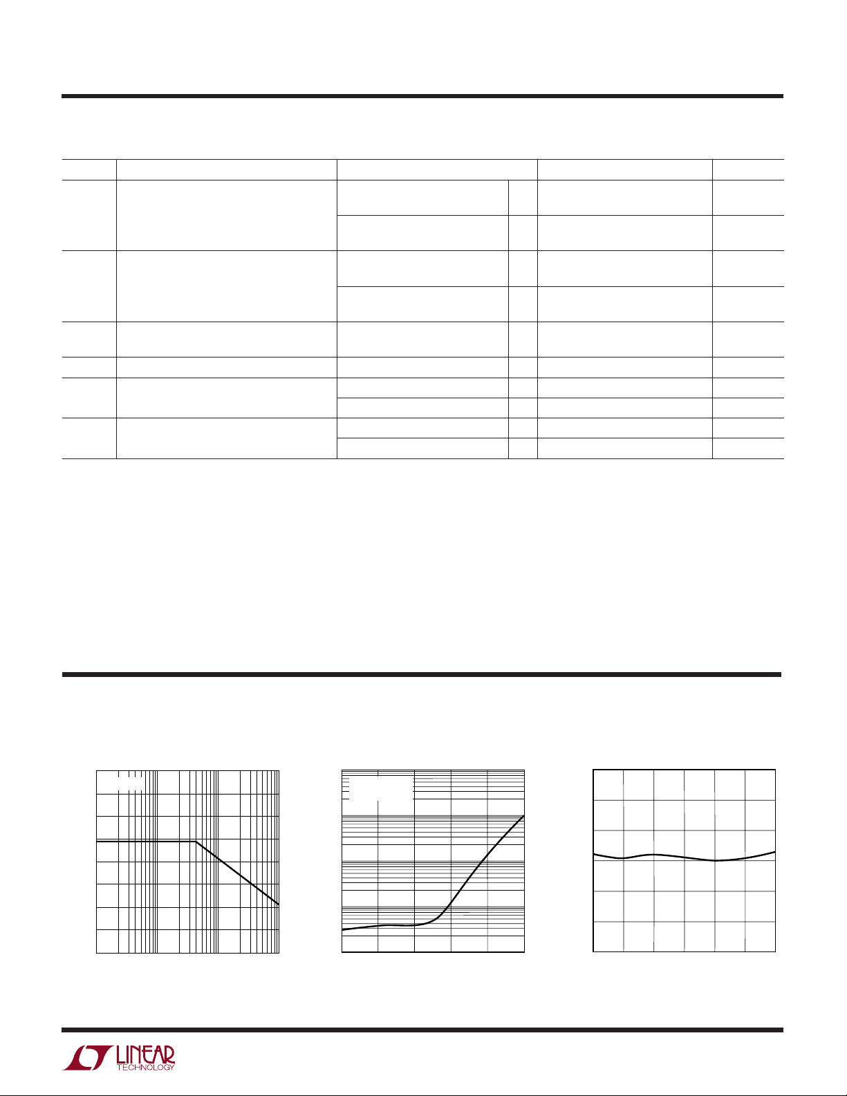
Ripple Rejection
CCHARA TERIST
ICS
UW
AT
Y
P
I
CA
LPER
F
O
R
C
E
FREQUENCY (Hz)
10
90
REJECTION (dB)
100
110
120
100
100 1k 10k
1027 G01
80
70
60
50
V
IN
= 10V
FREQUENCY (Hz)
0.01
OUTPUT IMPEDANCE (Ω)
0.1
1
10
100
10
10k
100k
1M
1027 G02
100
1k
∆I = ±3mA AC
I
SOURCE
= 5mA
Output Impedance vs Frequency
Output Voltage
TEMPERATURE (°C)
–50
OUTPUT VOLTAGE (V)
5.002
5.004
5.006
25 75
1027 G03
5.000
4.998
–25 0
50 100
4.996
4.994
E
LECTR
IC
AL C CHARA TERIST
ICS
The ● denotes specifications which apply over the full operating
temperature range otherwise specifications are at T
A
= 25°C. V
IN
= 10V, I
LOAD
= 0, unless otherwise specified.
器件 Datasheet 文档搜索
AiEMA 数据库涵盖高达 72,405,303 个元件的数据手册,每天更新 5,000 多个 PDF 文件
