Datasheet 搜索 > ADI(亚德诺) > LT1027CCS8-5#PBF 数据手册 > LT1027CCS8-5#PBF 产品设计参考手册 5/8 页

¥ 61.099
LT1027CCS8-5#PBF 产品设计参考手册 - ADI(亚德诺)
制造商:
ADI(亚德诺)
封装:
05-08-1610 (S8)
描述:
串联 15mA
Pictures:
3D模型
符号图
焊盘图
引脚图
产品图
页面导航:
典型应用电路图在P6
技术参数、封装参数在P3
应用领域在P6
导航目录
LT1027CCS8-5#PBF数据手册
Page:
of 8 Go
若手册格式错乱,请下载阅览PDF原文件
LT1027
5
sn1027 1027fcs
U
S
A
O
PP
L
IC
AT
I
WU
U
I FOR ATIO
to approximately 1.2µV
RMS
in a 10Hz to 1kHz bandwidth.
Transient response is not affected by this capacitor. Start-
up settling time will increase to several milliseconds due
to the 7kΩ impedance looking into the NR pin. The
capacitor
must
be a low leakage type. Electrolytics are
not
suitable for this application. Just 100nA leakage current
will result in a 150ppm error in output voltage. This pin is
the most sensitive pin on the device. For maximum protec-
tion a guard ring is recommended. The ring should be
driven from a resistive divider from V
OUT
set to 4.4V (the
open-circuit voltage on the NR pin).
Transient Response
The LT1027 has been optimized for transient response.
Settling time is under 2µs when an AC-coupled 10mA load
transient is applied to the output. The LT1027 achieves
fast settling by using a class B NPN/PNP output stage.
When sinking current, the device may oscillate with ca-
pacitive loads greater than 100pF. The LT1027 is stable
with all capacitive loads when at no DC load or when
sourcing current, although for best settling time either no
output bypass capactor or a 4.7µF tantalum unit is recom-
mended. An 0.1µF ceramic output capacitor will
maximize
output ringing
and is
not
recommended.
Kelvin Connections
Although the LT1027 does not have true force-sense
capability, proper hook-up can improve line loss and
ground loop problems significantly. Since the ground pin
of the LT1027 carries only 2mA, it can be used as a low-
side sense line, greatly reducing ground loop problems on
the low side of the reference. The V
OUT
pin should be close
to the load or connected via a heavy trace as the resistance
of this trace directly affects load regulation. It is important
to remember that a 1.22mV drop due to trace resistance is
equivalent to a 1LSB error in a 5V
FS
, 12-bit system.
The circuits in Figures 2 and 3 illustrate proper hook-up to
minimize errors due to ground loops and line losses.
Losses in the output lead can be further reduced by adding
a PNP boost transistor if load current is 5mA or higher. R2
can be added to further reduce current in the output sense
load.
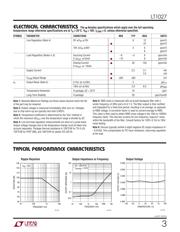
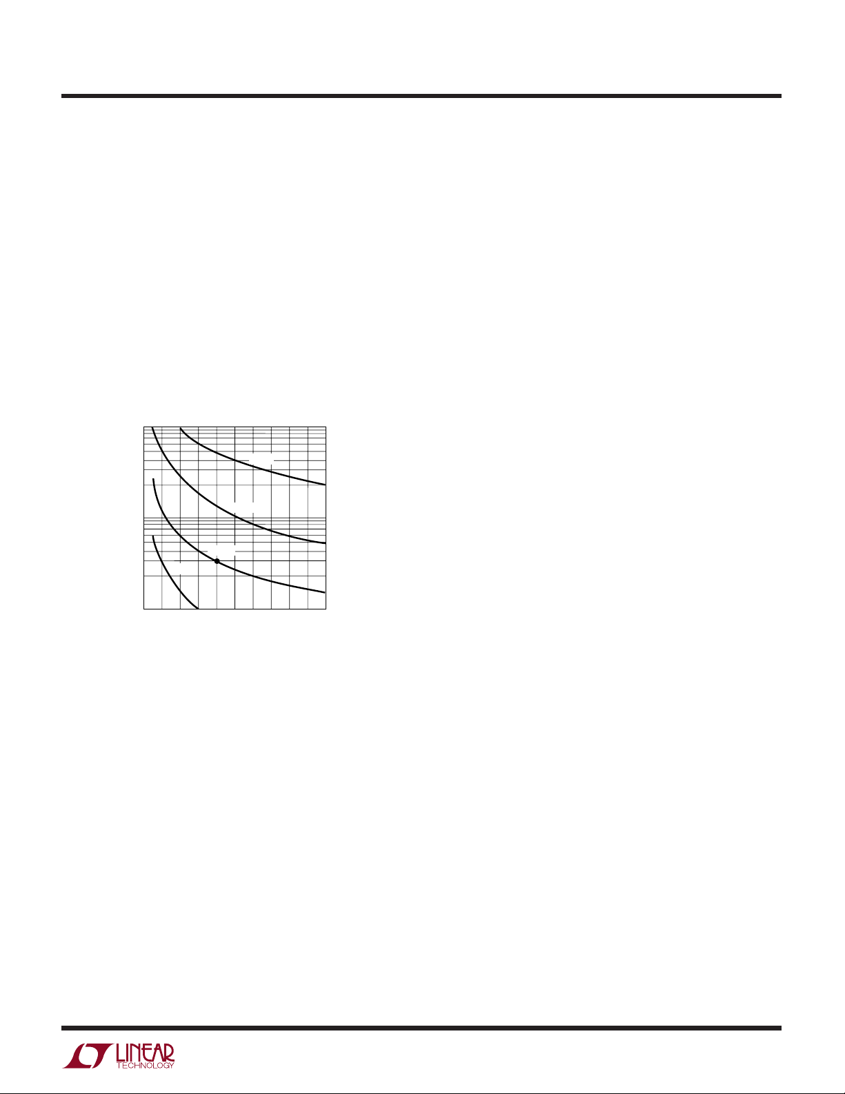
Effect of Reference Drift on System Accuracy
A large portion of the temperature drift error budget in
many systems is the system reference voltage. Figure 1
indicates the maximum temperature coefficient allowable
if the reference is to contribute no more than 0.5LSB error
to the overall system performance. The example shown is
a 12-bit system designed to operate over a temperature
range from 25°C to 65°C. Assuming the system calibra-
tion is performed at 25°C, the temperature span is 40°C.
It can be seen from the graph that the temperature coeffi-
cient of the reference must be no worse than 3ppm/°C if
it is to contribute less than 0.5LSB error. For this reason,
the LT1027 has been optimized for low drift.
Figure 1. Maximum Allowable Reference Drift
Trimming Output Voltage
The LT1027 has an adjustment pin for trimming output
voltage. The impedance of the V
ADJ
pin is about 20kΩ with
an open-circuit voltage of 2.5V. A ±30mV guaranteed trim
range is achievable by tying the V
ADJ
pin to the wiper of a
10k potentiometer connecting between the output and
ground. Trimming output voltage does not affect the TC of
the device.
Noise Reduction
The positive input of the internal scaling amplifier is
brought out as the Noise Reduction (NR) pin. Connecting
a 1µF Mylar capacitor between this pin and ground will
reduce the wideband noise of the LT1027 from 2.0µV
RMS
TEMPERATURE SPAN (°C)
100
MAXIMUM TEMPERATURE COEFFICIENT FOR
0.5LSB ERROR (ppm/°C)
30
100
1027 AI01
1.0
10
20 100
90
807060
50
40
8-BIT
10-BIT
12-BIT
14-BIT
器件 Datasheet 文档搜索
AiEMA 数据库涵盖高达 72,405,303 个元件的数据手册,每天更新 5,000 多个 PDF 文件
