Datasheet 搜索 > 稳压芯片 > ON Semiconductor(安森美) > NCP500SN27T1G 数据手册 > NCP500SN27T1G 产品设计参考手册 1/18 页

¥ 1.665
NCP500SN27T1G 产品设计参考手册 - ON Semiconductor(安森美)
制造商:
ON Semiconductor(安森美)
分类:
稳压芯片
封装:
TSOT-23-5
描述:
150mA,低功耗低压差稳压器
Pictures:
3D模型
符号图
焊盘图
引脚图
产品图
页面导航:
引脚图在P1Hot
典型应用电路图在P1P13
原理图在P1
封装尺寸在P17P18
焊盘布局在P17P18
型号编码规则在P1P16P18
标记信息在P1P16P18
封装信息在P16
功能描述在P2
技术参数、封装参数在P16
应用领域在P1P12P16
电气规格在P2P3P4P5P6
型号编号列表在P2
导航目录
NCP500SN27T1G数据手册
Page:
of 18 Go
若手册格式错乱,请下载阅览PDF原文件
© Semiconductor Components Industries, LLC, 2015
June, 2015 − Rev. 22
1 Publication Order Number:
NCP500/D
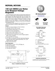
NCP500, NCV500
150 mA CMOS Low Noise
Low-Dropout Voltage
Regulator
The NCP500 series of fixed output low dropout linear regulators are
designed for portable battery powered applications which require low
noise operation, fast enable response time, and low dropout. The
device achieves its low noise performance without the need of an
external noise bypass capacitor. Each device contains a voltage
reference unit, an error amplifier, a PMOS power transistor, and
resistors for setting output voltage, and current limit and temperature
limit protection circuits.
The NCP500 has been designed to be used with low cost ceramic
capacitors and requires a minimum output capacitor of 1.0 mF.
Features
• Ultra−Low Dropout Voltage of 170 mV at 150 mA
• Fast Enable Turn−On Time of 20 msec
• Wide Operating Voltage Range of 1.8 V to 6.0 V
• Excellent Line and Load Regulation
• High Accuracy Output Voltage of 2.5%
• Enable Can Be Driven Directly by 1.0 V Logic
• Typical RMS Noise Voltage 50 mV with No Bypass Capacitor
(BW = 10 Hz to 100 kHz)
• Very Small DFN 2x2.2 Package
• NCV Prefix for Automotive and Other Applications Requiring
Unique Site and Control Change Requirements; AEC−Q100
Qualified and PPAP Capable
• These are Pb−Free Devices
Typical Applications
• Noise Sensitive Circuits − VCO’s, RF Stages, etc.
• SMPS Post−Regulation
• Hand−Held Instrumentation
• Camcorders and Cameras
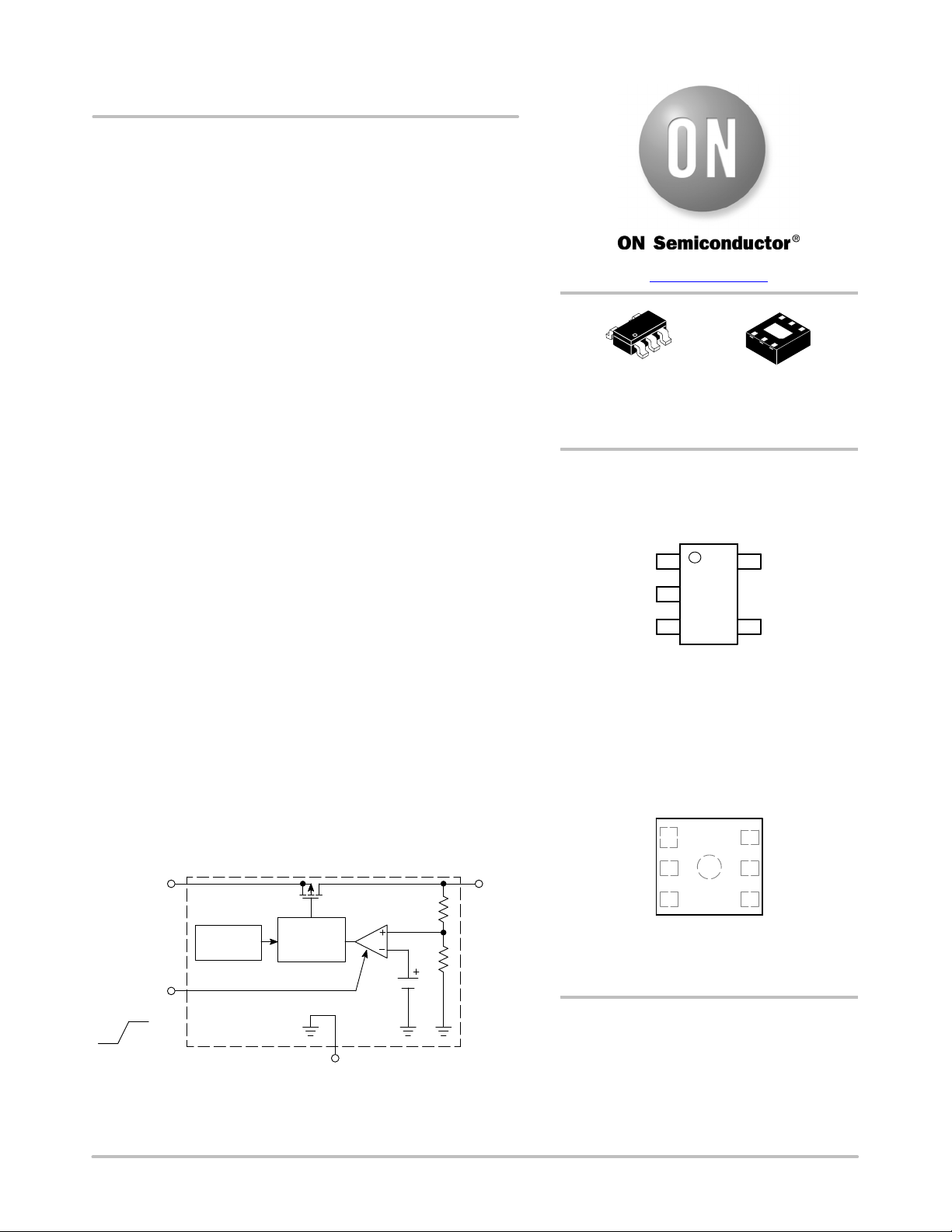
Driver w/
Current
Limit
V
in
V
out
Thermal
Shutdown
Enable
GND
OFF
ON
1 (3)
3 (1)
5 (4)
2 (2, 5)
Figure 1. Simplified Block Diagram
NOTE: Pin numbers in parenthesis indicate DFN package.
See detailed ordering and shipping information in the package
dimensions section on page 16 of this data sheet.
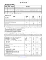
ORDERING INFORMATION
TSOP−5
SN SUFFIX
CASE 483
1
5
PIN CONNECTIONS AND
MARKING DIAGRAMS
1
3
N/C
V
in
2GND
Enable
4
V
out
5
xxx = Specific Device Code
A = Assembly Location
Y = Year
W = Work Week
G = Pb−Free Package
(Note: Microdot may be in either location)
(Top View)
TSOP−5
DFN 2x2.2 MM
SQL SUFFIX
CASE 506BA
1
3
N/C
V
in
2
GND
Enable
4
V
out
5
6
GND
(Top View)
www.onsemi.com
xxM
xxxAYWG
G
DFN 2x2.2 mm
xx = Specific Device Code
M = Date Code
1
6
器件 Datasheet 文档搜索
AiEMA 数据库涵盖高达 72,405,303 个元件的数据手册,每天更新 5,000 多个 PDF 文件
