Datasheet 搜索 > 稳压芯片 > ON Semiconductor(安森美) > NCP500SN27T1G 数据手册 > NCP500SN27T1G 产品设计参考手册 3/18 页

¥ 1.665
NCP500SN27T1G 产品设计参考手册 - ON Semiconductor(安森美)
制造商:
ON Semiconductor(安森美)
分类:
稳压芯片
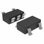
封装:
TSOT-23-5
描述:
150mA,低功耗低压差稳压器
Pictures:
3D模型
符号图
焊盘图
引脚图
产品图
页面导航:
引脚图在P1Hot
典型应用电路图在P1P13
原理图在P1
封装尺寸在P17P18
焊盘布局在P17P18
型号编码规则在P1P16P18
标记信息在P1P16P18
封装信息在P16
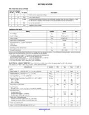
功能描述在P2
技术参数、封装参数在P16
应用领域在P1P12P16
电气规格在P2P3P4P5P6
型号编号列表在P2
导航目录
NCP500SN27T1G数据手册
Page:
of 18 Go
若手册格式错乱,请下载阅览PDF原文件
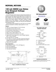
NCP500, NCV500
www.onsemi.com
3
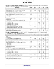
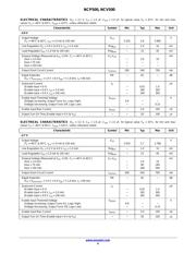
ELECTRICAL CHARACTERISTICS (continued) (V
in
= 2.35 V, C
in
= 1.0 mF, C
out
= 1.0 mF, for typical value T
A
= 25°C, for min and
max values T
A
= −40°C to 85°C, T
jmax
= 125°C, unless otherwise noted)
Characteristic
Symbol Min Typ Max Unit
−1.85 V
Output Voltage (T
A
= −40°C to 85°C, I
out
= 1.0 mA to 150 mA) V
out
1.804 1.85 1.896 V
Line Regulation (V
in
= 2.3 V to 6.0 V, I
out
= 1.0 mA) Reg
line
− 1.0 10 mV
Load Regulation (I
out
= 1.0 mA to 150 mA) Reg
load
− 15 45 mV
Dropout Voltage (Measured at V
out
−2.0%, T
A
= −40°C to 85°C)
(Iout = 1.0 mA)
(Iout = 75 mA)
(Iout = 150 mA)
V
in
−V
out
−
−
−
2.0
−
−
10
−
−
mV
Output Short Circuit Current I
out(max)
200 540 700 mA
Ripple Rejection
(V
in
= V
out
(nom.)
+ 1.0 V + 0.5 V
pp
, f = 1.0 kHz, I
o
= 60 mA)
RR − 62 − dB
Quiescent Current
(Enable Input = 0 V)
(Enable Input = 0.9 V, I
out
= 1.0 mA)
(Enable Input = 0.9 V, I
out
= 150 mA)
I
Q
−
−
−
0.01
175
175
1.0
300
300
mA
Enable Input Threshold Voltage
(Voltage Increasing, Output Turns On, Logic High)
(Voltage Decreasing, Output Turns Off, Logic Low)
V
th(EN)
0.9
−
−
−
−
0.15
V
Enable Input Bias Current I
IB(EN)
− 3.0 100 nA
Output Turn On Time (Enable Input = 0 V to V
in
) − − 20 100
ms
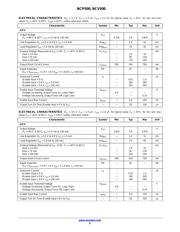
ELECTRICAL CHARACTERISTICS (V
in
= 3.0 V, C
in
= 1.0 mF, C
out
= 1.0 mF, for typical value T
A
= 25°C, for min and max values
T
A
= −40°C to 85°C, T
jmax
= 125°C, unless otherwise noted)
Characteristic
Symbol Min Typ Max Unit
−2.5 V
Output Voltage
(T
A
=−40°C to 85°C, I
out
= 1.0 mA to 150 mA)
V
out
2.438 2.5 2.563
V
Line Regulation (V
in
= 3.0 V to 6.0 V, I
out
= 1.0 mA) Reg
line
− 1.0 10 mV
Load Regulation (I
out
= 1.0 mA to 150 mA) Reg
load
− 15 45 mV
Dropout Voltage (Measured at V
out
−2.0%, T
A
= −40°C to 85°C)
(Iout = 1.0 mA)
(Iout = 75 mA)
(Iout = 150 mA)
V
in
−V
out
−
−
−
2.0
100
190
10
170
270
mV
Output Short Circuit Current I
out(max)
200 540 700 mA
Ripple Rejection
(V
in
= V
out
(nom.)
+ 1.0 V + 0.5 V
pp
, f = 1.0 kHz, I
o
= 60 mA)
RR − 62 − dB
Quiescent Current
(Enable Input = 0 V)
(Enable Input = 0.9 V, I
out
= 1.0 mA)
(Enable Input = 0.9 V, I
out
= 150 mA)
I
Q
−
−
−
0.01
180
180
1.0
300
300
mA
Enable Input Threshold Voltage
(Voltage Increasing, Output Turns On, Logic High)
(Voltage Decreasing, Output Turns Off, Logic Low)
V
th(EN)
0.9
−
−
−
−
0.15
V
Enable Input Bias Current I
IB(EN)
− 3.0 100 nA
Output Turn On Time (Enable Input = 0 V to V
in
) − − 20 100
ms
器件 Datasheet 文档搜索
AiEMA 数据库涵盖高达 72,405,303 个元件的数据手册,每天更新 5,000 多个 PDF 文件
