Datasheet 搜索 > JFET晶体管 > ON Semiconductor(安森美) > MMBFJ111 数据手册 > MMBFJ111 用户编程技术手册 2/5 页

¥ 0.586
MMBFJ111 用户编程技术手册 - ON Semiconductor(安森美)
制造商:
ON Semiconductor(安森美)
分类:
JFET晶体管
封装:
SOT-23-3
描述:
MMBF系列 N沟道 35 V 20 mA 表面贴装 低噪声 放大器 开关 - SOT-23-3
Pictures:
3D模型
符号图
焊盘图
引脚图
产品图
页面导航:
型号编码规则在P5
标记信息在P1P5

导航目录
MMBFJ111数据手册
Page:
of 5 Go
若手册格式错乱,请下载阅览PDF原文件
www.fairchildsemi.com
© 1977 Fairchild Semiconductor Corporation www.fairchildsemi.com
Rev. 1.0 • 7/16/15
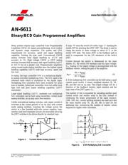
AN-6611
Binary/BCD Gain Programmed Amplifiers
Many systems require logic controlled Gain Programmable
Amplifiers (GPA) for signal preconditioning, level control
and dynamic range expansion. The system sets GPA
requirements for accuracy, speed and signal handling
capability, limiting the type used. Conventional CMOS
analog switches limit signal handling to ±7.5 V and
accuracy to 1%. High voltage CMOS or JFET analog
switches increase both accuracy and signal handling (±10 V
to ±15 V) but at a greater cost. Programmable amplifiers
using current mode analog switches have the highest signal
handling capability (±25 V) with high accuracy, speed and
low cost.
In reality, the logic controlled GPA is a multiplying digital-
to-analog converter (multiplying D/A). The D/A input is the
reference node which is multiplied by the digital input.
Multiplying D/A converters have been available for some
time in module, hybrid and monolithic form but suffer from
high cost and poor signal handling capability (±10 V
maximum).
Large signal handling (±25 V), moderate cost multiplying
D/A converters can be built using monolithic current mode
analog switches, an op amp and a few resistors.
Unlike conventional analog switches, only signal current is
switched at the virtual ground of an op amp with current
mode analog switches. Limiting the voltage across the
switch to a few hundred millivolts, power supplies, logic
interface and level translator circuits are eliminated allowing
the JFET switches to be driven directly by standard logic.
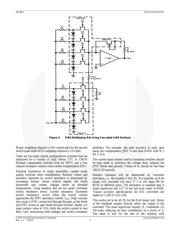
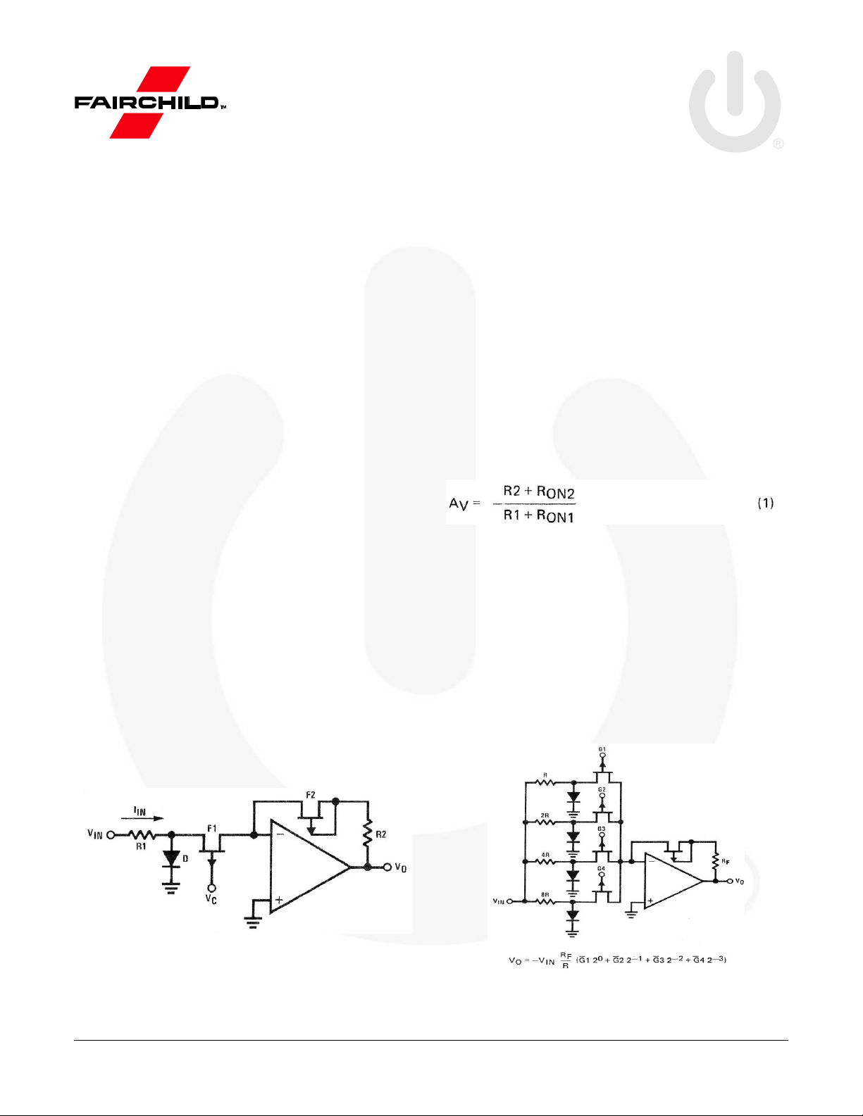
Figure 1. Current Mode Analog Switch
A logic "0" turns the switch ON with a logic "1" shutting the
switch OFF by pinching the JFET OFF. The diode is used to
clamp the source to drain voltage to about 0.7 V in the
switch OFF state. The series JFET in the feedback path is
used to compensate for the ON resistance of the switch
JFET.
Current through the switch is determined by the input
resistor, R1, the switch ON resistance and the input voltage,
V
IN
. Scaling of the output voltage is accomplished with the
feedback resistor, setting the gain of the amplifier.
A 4-bit multiplying D/A converter can be built using a quad
current mode switch, 4 binary weighted resistors (R, 2R,
4R, and 8R) and an op amp. The output voltage will be a
function of the feedback resistor, input resistors and the
logic state of the JFET gates, G
N
.
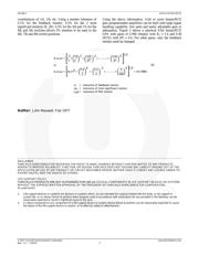
The number of bits is expanded by cascading another quad
current switch and resistor array to the first. Instead of
continuing the binary progression of the input resistors,
(16R, 32R, etc), current splitting resistors are used such that
the same resistor array (R, 2R, 4R, 8R) is used for the
additional bits, minimizing the number of resistor values
required for higher order converters.
Figure 2. 4-Bit Multiplying D/A Converter
器件 Datasheet 文档搜索
AiEMA 数据库涵盖高达 72,405,303 个元件的数据手册,每天更新 5,000 多个 PDF 文件
