Datasheet 搜索 > JFET晶体管 > ON Semiconductor(安森美) > MMBFJ111 数据手册 > MMBFJ111 用户编程技术手册 3/5 页

¥ 0.586
MMBFJ111 用户编程技术手册 - ON Semiconductor(安森美)
制造商:
ON Semiconductor(安森美)
分类:
JFET晶体管
封装:
SOT-23-3
描述:
MMBF系列 N沟道 35 V 20 mA 表面贴装 低噪声 放大器 开关 - SOT-23-3
Pictures:
3D模型
符号图
焊盘图
引脚图
产品图
页面导航:
型号编码规则在P5
标记信息在P1P5

导航目录
MMBFJ111数据手册
Page:
of 5 Go
若手册格式错乱,请下载阅览PDF原文件
AN-6611 APPLICATION NOTE
© 1977 Fairchild Semiconductor Corporation www.fairchildsemi.com
Rev. 1.0 • 7/16/15 2
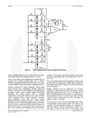
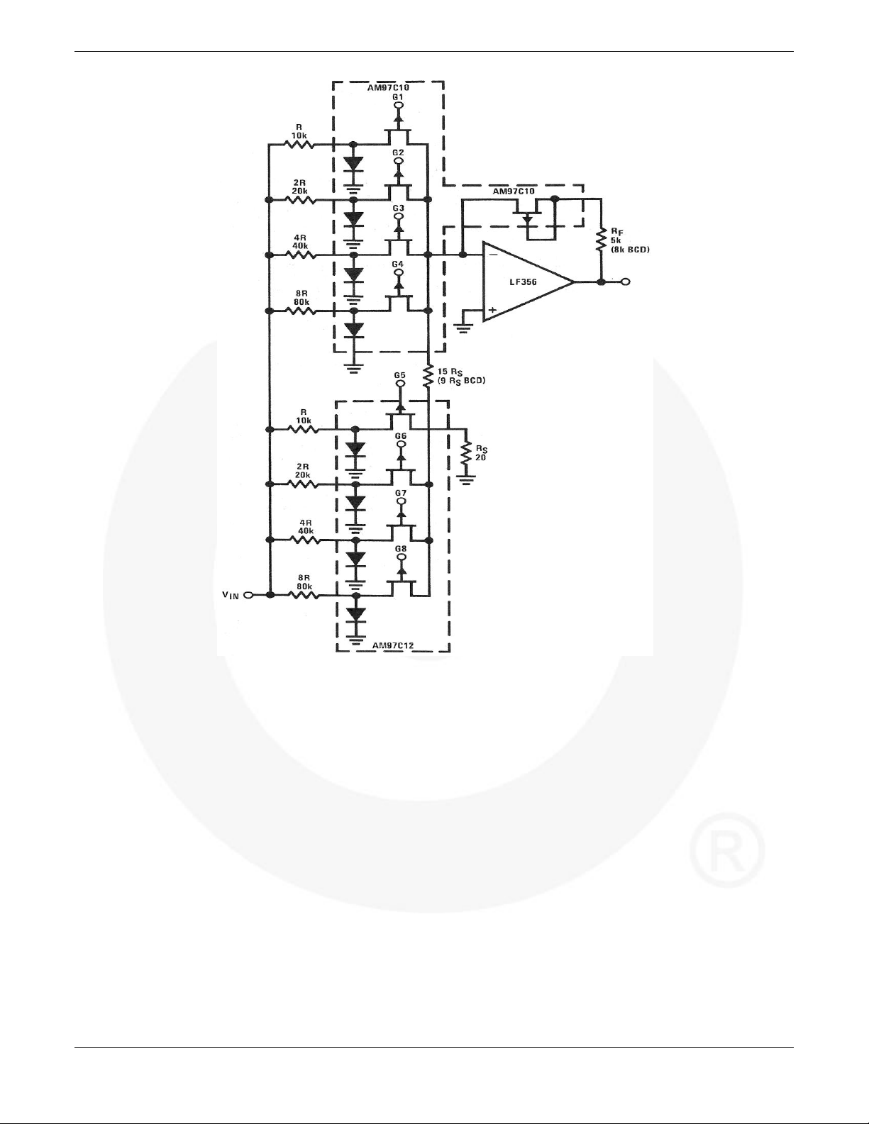
Figure 3. 8-Bit Multiplying D/A Using Cascaded 4-Bit Sections
Binary weighting requires a 1/16 current split for the second
switch quad while BCD weighting requires a 1/10 split.
There are two basic switch configurations available that are
optimized for a variety of logic drives: TTL or CMOS
Multiple independent switches (four by SPST) and a four
channel multiplex version with a series compensation JFET.
Practical limitations in using monolithic current mode
analog switches need consideration. Resistor values and
tolerance impacted by switch resistance is minimized by
increasing resistor values without regard, but limits
bandwidth and creates leakage errors at elevated
temperatures. Using resistors that are too small, increases
switch resistance errors. Current saturation (increased
switch resistance) occurs when the switch current
approaches the JFET saturation current, I
DSS
. High currents
also cause I
G
(ON), current lost through the gate, as the diode
and JFET source to gate diode become forward biased. An
input resistor value of 10 k limits the switch current to less
than 2 mA minimizing both leakage and switch resistance
problems. For example, the gain accuracy at unity gain
using the compensation JFET is less than 0.05% with R =
RF = 10 k.
The current shunt resistor used in cascading switches should
be kept small to minimize the voltage drop, keeping the
JFET drains near ground. Values of R
S
should be less than
100 (20 typical).
Resistor tolerance will be determined by converter
resolution, i.e., the number if bits (N). For example, an 8-bit
binary D/A converter will have 2
N
-1 or 255 steps (99 for
BCD) or different gains. The resolution or smallest step is
(least significant bit) 1/2
N
of the full-scale value (0.0039).
Typical accuracy specifications for D/A converters are
stated as 1 LSB or ±1/2 LSB.
This works out to be ±0.2% for the 8-bit binary unit. Errors
in the feedback resistor directly affect the output of the
converter. The most significant resistor, R, contributes 1/2
full-scale, reducing its error contribution by a factor of 2.
The same is true for the rest of the resistors with
器件 Datasheet 文档搜索
AiEMA 数据库涵盖高达 72,405,303 个元件的数据手册,每天更新 5,000 多个 PDF 文件
