Datasheet 搜索 > 特殊应用集成芯片 > ADI(亚德诺) > ADE7763ARSZ 数据手册 > ADE7763ARSZ 开发手册 4/16 页
 器件3D模型
¥ 10.395
ADE7763ARSZ 开发手册 - ADI(亚德诺)
制造商:
ADI(亚德诺)
分类:
特殊应用集成芯片
封装:
SSOP-20
描述:
ANALOG DEVICES ADE7763ARSZ. 芯片, 能量计, 单相, SSOP-20
Pictures:
3D模型
符号图
焊盘图
引脚图
产品图
页面导航:
型号编码规则在P1
应用领域在P16
电气规格在P7

导航目录
ADE7763ARSZ数据手册
Page:
of 16 Go
若手册格式错乱,请下载阅览PDF原文件
AN-639 Application Note
Rev. A | Page 4 of 16
Table 1. Sensor Technologies
Sensor Benefits Drawbacks
Low
Resistance
Shunt
Very low cost,
good linearity
Poor high current
capability, dc offset,
parasitic inductance
Current
Transformer
Good high current
performance,
low power
consumption
Hysteresis/saturation due
to dc, phase shift,
susceptible to external
magnetic fields
Hall Effect
Sensor
Good high current
performance,
wide dynamic range
Hysteresis/saturation,
higher cost, temperature
drift
Rogowski
Coil
(Air-Core CT)
Low cost,
no saturation limit,
low power consumption,
immunity to dc offset,
wide dynamic range,
very low temperature
range
Output is derivative of
voltage signal—requires
an analog (or digital)
integrator.
EMI sensitivity.
Many ADE ICs have a built-in digital integrator for easy
interface with a Rogowski coil. In all cases, the integrator can
be turned off to interface with a current transformer (CT)
or shunt.
What are the considerations for selecting the shunt?
The following are several main considerations for the shunt:
• Thermal management consideration. For a large (high
resistance) shunt, there will be significant temperature rise
if the current is large.
• Shunt quality. The self-heating of the shunt can increase its
resistance. The output signal can vary because of this, and
affects the accuracy of the meter.
• Tampering consideration. The resistance of the shunt
should be as close to a wire as possible to minimize the
effect of any attempt to divert the current using an external
wire.
• Signal level. The shunt should provide reasonable signal
levels to the IC over the current operation range.
• Power consumption requirement. According to IEC 61036,
the power consumption per channel cannot exceed 2 W.
Larger shunts consume more power.
What are the considerations for selecting a current
transformer (CT)?
Care should be taken to ensure that the dynamic range for
current sensing with a given CT is large enough for the
application. Current transformers can saturate under large dc
or high current, and designers should choose CTs rated for their
needs. CTs can introduce phase shift and should be chosen
according to the designer’s ability to compensate for this error.
In addition, note that certain CTs introduce an inherent scaling
error depending on the turns ratio selected and, thus, care must
be taken to ensure that the current level at the secondary of the
CT is the same as expected.
How do I compensate for the phase shift of my current
sensor?
The internal PHCAL register can be used in all ADE products
(except ADE7761B, ADE7757A, ADE7768, ADE7769,
ADE7751, ADE7755, ADE7762, and ADE7752A) to adjust
the phase lead/lag. Adjusting the phase mismatch is a simple
procedure of writing to the register. Refer to the specific data
sheet for details. If the compensation range is beyond that of
the PHCAL register, a combination of both hardware and
software phase adjustment can be used. For example, you can
use the hardware method to roughly compensate the default
phase mismatch and use the PHCAL register as a fine
adjustment in production. If a hardware method is required,
the phase mismatch at the line frequency can be corrected by
adjusting the corner frequency of the RC filter (used for
antialiasing on the input channels) to create a phase shift that
would offset the phase error. The AN-563
Application Note
provides a detailed description of how to adjust the phase
mismatch.
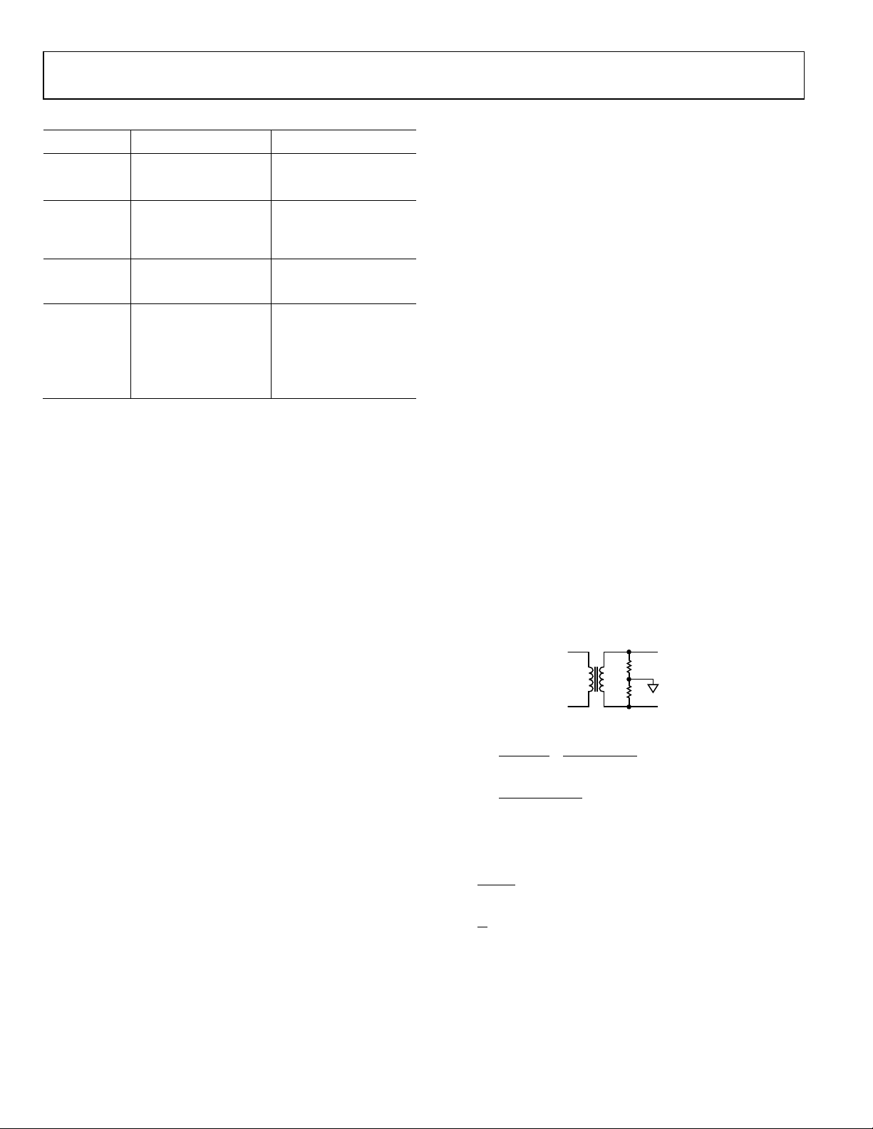
How do I calculate the burden resistor to use with my
current transformer?
The burden resistor depends on the maximum current (I
MAX
),
the input level to the ADC (y), and the number of turns in the
CT being used (CTRN). At maximum current, the input signal
at the current channel should be at half input full scale to allow
headroom. The full scale can be 660 mV p-p, 500 mV p-p, or
1 V p-p, depending on the product. Refer to the product data
sheet for specifications. Assuming that the 5750:1 CT is center-
tapped as shown in the Figure 2, the burden resistor can be
calculated as shown in Figure 2.
Figure 2. CT with Center-Tapped Burden Resistors
y =
2
peakmV500
2
=
FullScale
=
2
rmsmV55.353
= 176.8 mV rms
The following equations apply:
x
CTRN
Imax
=
b
R
x
y
2=
where CTRN= 5750.
Solve for R
b
. For example, if I
MAX
is 113.1 A rms, R
b
= 4.5 Ω.
It is recommended to use a center-tapped burden as shown in
Figure 2. If the burden resistor is not center-tapped as shown in
R
b
R
b
03598-002
器件 Datasheet 文档搜索
AiEMA 数据库涵盖高达 72,405,303 个元件的数据手册,每天更新 5,000 多个 PDF 文件
