Datasheet 搜索 > MOS管 > ON Semiconductor(安森美) > 2N7002KT1G 数据手册 > 2N7002KT1G 数据手册 6/7 页

¥ 0.116
2N7002KT1G 数据手册 - ON Semiconductor(安森美)
制造商:
ON Semiconductor(安森美)
分类:
MOS管
封装:
SOT-23-3
描述:
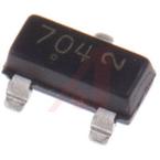
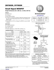
ON SEMICONDUCTOR 2N7002KT1G. 场效应管, MOSFET, N沟道, 60V, 380mA SOT-23
Pictures:
3D模型
符号图
焊盘图
引脚图
产品图
2N7002KT1G数据手册
Page:
of 7 Go
若手册格式错乱,请下载阅览PDF原文件
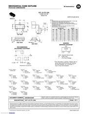
SOT−23 (TO−236)
CASE 318−08
ISSUE AS
DATE 30 JAN 2018
SCALE 4:1
D
A1
3
1
2
1
XXXMG
G
XXX = Specific Device Code
M = Date Code
G = Pb−Free Package
*This information is generic. Please refer to
device data sheet for actual part marking.
Pb−Free indicator, “G” or microdot “ G”,
may or may not be present.
GENERIC
MARKING DIAGRAM*
NOTES:
1. DIMENSIONING AND TOLERANCING PER ASME Y14.5M, 1994.
2. CONTROLLING DIMENSION: MILLIMETERS.
3. MAXIMUM LEAD THICKNESS INCLUDES LEAD FINISH.
MINIMUM LEAD THICKNESS IS THE MINIMUM THICKNESS OF
THE BASE MATERIAL.
4. DIMENSIONS D AND E DO NOT INCLUDE MOLD FLASH,
PROTRUSIONS, OR GATE BURRS.
SOLDERING FOOTPRINT
VIEW C
L
0.25
L1
e
E
E
b
A
SEE VIEW C
DIM
A
MIN NOM MAX MIN
MILLIMETERS
0.89 1.00 1.11 0.035
INCHES
A1 0.01 0.06 0.10 0.000
b 0.37 0.44 0.50 0.015
c 0.08 0.14 0.20 0.003
D 2.80 2.90 3.04 0.110
E 1.20 1.30 1.40 0.047
e 1.78 1.90 2.04 0.070
L 0.30 0.43 0.55 0.012
0.039 0.044
0.002 0.004
0.017 0.020
0.006 0.008
0.114 0.120
0.051 0.055
0.075 0.080
0.017 0.022
NOM MAX
L1
H
STYLE 22:
PIN 1. RETURN
2. OUTPUT
3. INPUT
STYLE 6:
PIN 1. BASE
2. EMITTER
3. COLLECTOR
STYLE 7:
PIN 1. EMITTER
2. BASE
3. COLLECTOR
STYLE 8:
PIN 1. ANODE
2. NO CONNECTION
3. CATHODE
STYLE 9:
PIN 1. ANODE
2. ANODE
3. CATHODE
STYLE 10:
PIN 1. DRAIN
2. SOURCE
3. GATE
STYLE 11:
PIN 1. ANODE
2. CATHODE
3. CATHODE−ANODE
STYLE 12:
PIN 1. CATHODE
2. CATHODE
3. ANODE
STYLE 13:
PIN 1. SOURCE
2. DRAIN
3. GATE
STYLE 14:
PIN 1. CATHODE
2. GATE
3. ANODE
STYLE 15:
PIN 1. GATE
2. CATHODE
3. ANODE
STYLE 16:
PIN 1. ANODE
2. CATHODE
3. CATHODE
STYLE 17:
PIN 1. NO CONNECTION
2. ANODE
3. CATHODE
STYLE 18:
PIN 1. NO CONNECTION
2. CATHODE
3. ANODE
STYLE 19:
PIN 1. CATHODE
2. ANODE
3. CATHODE−ANODE
STYLE 23:
PIN 1. ANODE
2. ANODE
3. CATHODE
STYLE 20:
PIN 1. CATHODE
2. ANODE
3. GATE
STYLE 21:
PIN 1. GATE
2. SOURCE
3. DRAIN
STYLE 1 THRU 5:
CANCELLED
STYLE 24:
PIN 1. GATE
2. DRAIN
3. SOURCE
STYLE 25:
PIN 1. ANODE
2. CATHODE
3. GATE
STYLE 26:
PIN 1. CATHODE
2. ANODE
3. NO CONNECTION
STYLE 27:
PIN 1. CATHODE
2. CATHODE
3. CATHODE
2.10 2.40 2.64 0.083 0.094 0.104
H
E
0.35 0.54 0.69 0.014 0.021 0.027
c
0 −−− 10 0 −−− 10
T
°°°°
T
3X
TOP VIEW
SIDE VIEW
END VIEW
2.90
0.80
DIMENSIONS: MILLIMETERS
0.90
PITCH
3X
3X
0.95
RECOMMENDED
STYLE 28:
PIN 1. ANODE
2. ANODE
3. ANODE
MECHANICAL CASE OUTLINE
PACKAGE DIMENSIONS
ON Semiconductor and are trademarks of Semiconductor Components Industries, LLC dba ON Semiconductor or its subsidiaries in the United States and/or other countries.
ON Semiconductor reserves the right to make changes without further notice to any products herein. ON Semiconductor makes no warranty, representation or guarantee regarding
the suitability of its products for any particular purpose, nor does ON Semiconductor assume any liability arising out of the application or use of any product or circuit, and specifically
disclaims any and all liability, including without limitation special, consequential or incidental damages. ON Semiconductor does not convey any license under its patent rights nor the
rights of others.
98ASB42226B
DOCUMENT NUMBER:
DESCRIPTION:
Electronic versions are uncontrolled except when accessed directly from the Document Repository.
Printed versions are uncontrolled except when stamped “CONTROLLED COPY” in red.
PAGE 1 OF 1
SOT−23 (TO−236)
© Semiconductor Components Industries, LLC, 2019
www.onsemi.com
Downloaded from Arrow.com.Downloaded from Arrow.com.Downloaded from Arrow.com.Downloaded from Arrow.com.Downloaded from Arrow.com.Downloaded from Arrow.com.
器件 Datasheet 文档搜索
AiEMA 数据库涵盖高达 72,405,303 个元件的数据手册,每天更新 5,000 多个 PDF 文件
