Datasheet 搜索 > Intel(英特尔) > 5AGXFB3H4F35I3 数据手册 > 5AGXFB3H4F35I3 数据手册 27/183 页


¥ 15672.423
5AGXFB3H4F35I3 数据手册 - Intel(英特尔)
制造商:
Intel(英特尔)
封装:
BGA
Pictures:
3D模型
符号图
焊盘图
引脚图
产品图
页面导航:
引脚图在P10P11P19P27P31Hot
技术参数、封装参数在P4P5P14P15P16P18P19P21P22P25P26P27
电气规格在P4P104
导航目录
5AGXFB3H4F35I3数据手册
Page:
of 183 Go
若手册格式错乱,请下载阅览PDF原文件
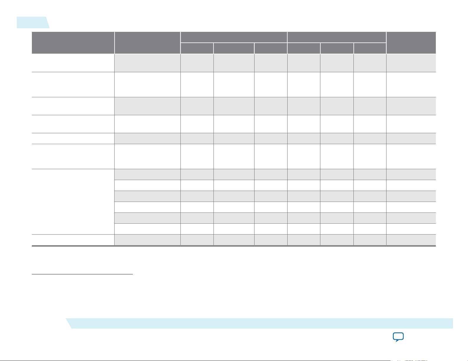
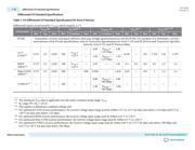
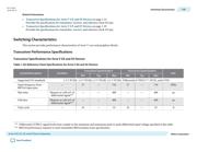
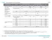
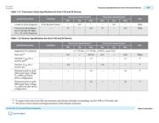
Symbol/Description Condition
Transceiver Speed Grade 4 Transceiver Speed Grade 6
Unit
Min Typ Max Min Typ Max
Peak-to-peak differential
input voltage
— 200 — 300
(25)
/
2000
200 — 300
(25)
/
2000
mV
Spread-spectrum
modulating clock
frequency
PCI Express
®
(PCIe) 30 — 33 30 — 33 kHz
Spread-spectrum
downspread
PCIe — 0 to –0.5% — — 0 to –0.5% — —
On-chip termination
resistors
— — 100 — — 100 — Ω
V
ICM
(AC coupled) — — 1.1/1.15
(26)
— — 1.1/1.15
(26)
— V
V
ICM
(DC coupled) HCSL I/O standard for
the PCIe reference
clock
250 — 550 250 — 550 mV
Transmitter REFCLK phase
noise
(27)
10 Hz — — –50 — — –50 dBc/Hz
100 Hz — — –80 — — –80 dBc/Hz
1 KHz — — –110 — — –110 dBc/Hz
10 KHz — — –120 — — –120 dBc/Hz
100 KHz — — –120 — — –120 dBc/Hz
≥1 MHz — — –130 — — –130 dBc/Hz
R
REF
— — 2000 ±1% — — 2000 ±1% — Ω
(25)
The maximum peak-to peak differential input voltage of 300 mV is allowed for DC coupled link.
(26)
For data rate ≤3.2 Gbps, connect V
CCR_GXBL/R
to either 1.1-V or 1.15-V power supply. For data rate >3.2 Gbps, connect V
CCR_GXBL/R
to a 1.15-V
power supply. For details, refer to the Arria V GT, GX, ST, and SX Device Family Pin Connection Guidelines.
(27)
The transmitter REFCLK phase jitter is 30 ps p-p at bit error rate (BER) 10
-12
.
1-24
Transceiver Specifications for Arria V GX and SX Devices
AV-51002
2016.06.10
Altera Corporation
Arria V GX, GT, SX, and ST Device Datasheet
Send Feedback
器件 Datasheet 文档搜索
AiEMA 数据库涵盖高达 72,405,303 个元件的数据手册,每天更新 5,000 多个 PDF 文件
