Datasheet 搜索 > FPGA芯片 > Altera(阿尔特拉) > 5AGXFB3H4F35I3G 数据手册 > 5AGXFB3H4F35I3G 数据手册 19/183 页
 器件3D模型
¥ 18588.172
5AGXFB3H4F35I3G 数据手册 - Altera(阿尔特拉)
制造商:
Altera(阿尔特拉)
分类:
FPGA芯片
封装:
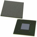
BBGA-1152
描述:
FPGA - 现场可编程门阵列
Pictures:
3D模型
符号图
焊盘图
引脚图
产品图
页面导航:
引脚图在P10P11P19P27P31Hot
技术参数、封装参数在P4P5P14P15P16P18P19P21P22P25P26P27
电气规格在P4P104
导航目录
5AGXFB3H4F35I3G数据手册
Page:
of 183 Go
若手册格式错乱,请下载阅览PDF原文件
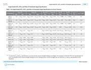
Symbol Description Maximum Unit
I
XCVR-TX (DC)
DC current per transceiver transmitter (TX) pin 100 mA
I
XCVR-RX (DC)
DC current per transceiver receiver (RX) pin 50 mA
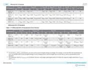
Internal Weak Pull-Up Resistor
All I/O pins, except configuration, test, and JTAG pins, have an option to enable weak pull-up.
Table 1-13: Internal Weak Pull-Up Resistor Values for Arria V Devices
Symbol Description Condition (V)
(11)
Value
(12)
Unit
R
PU
Value of the I/O pin pull-up resistor before and during
configuration, as well as user mode if you have enabled the
programmable pull-up resistor option.
V
CCIO
= 3.3 ±5% 25 kΩ
V
CCIO
= 3.0 ±5% 25 kΩ
V
CCIO
= 2.5 ±5% 25 kΩ
V
CCIO
= 1.8 ±5% 25 kΩ
V
CCIO
= 1.5 ±5% 25 kΩ
V
CCIO
= 1.35 ±5% 25 kΩ
V
CCIO
= 1.25 ±5% 25 kΩ
V
CCIO
= 1.2 ±5% 25 kΩ
Related Information
Arria V GT, GX, ST, and SX Device Family Pin Connection Guidelines
Provides more information about the pins that support internal weak pull-up and internal weak pull-down features.
I/O Standard Specifications
Tables in this section list the input voltage (V
IH
and V
IL
), output voltage (V
OH
and V
OL
), and current drive characteristics (I
OH
and I
OL
) for various
I/O standards supported by Arria V devices.
(11)
Pin pull-up resistance values may be lower if an external source drives the pin higher than V
CCIO
.
(12)
Valid with ±10% tolerances to cover changes over PVT.
1-16
Internal Weak Pull-Up Resistor
AV-51002
2016.06.10
Altera Corporation
Arria V GX, GT, SX, and ST Device Datasheet
Send Feedback
器件 Datasheet 文档搜索
AiEMA 数据库涵盖高达 72,405,303 个元件的数据手册,每天更新 5,000 多个 PDF 文件
