Datasheet 搜索 > 电压电平转换器 > NXP(恩智浦) > 74AVC8T245BQ,118 数据手册 > 74AVC8T245BQ,118 数据手册 4/24 页

¥ 7.264
74AVC8T245BQ,118 数据手册 - NXP(恩智浦)
制造商:
NXP(恩智浦)
分类:
电压电平转换器
封装:
VFQFN-24
描述:
74AVC 系列 3.6 V 3态 8-位 双电源转换 收发器 - DHVQFN-24
Pictures:
3D模型
符号图
焊盘图
引脚图
产品图
页面导航:
导航目录
74AVC8T245BQ,118数据手册
Page:
of 24 Go
若手册格式错乱,请下载阅览PDF原文件
74AVC8T245 All information provided in this document is subject to legal disclaimers. © NXP B.V. 2012. All rights reserved.
Product data sheet Rev. 5 — 27 December 2012 4 of 24
NXP Semiconductors
74AVC8T245
8-bit dual supply translating transceiver; 3-state
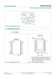
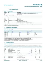
5.2 Pin description
[1] All GND pins must be connected to ground (0 V).
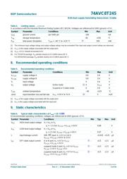
6. Functional description
[1] H = HIGH voltage level; L = LOW voltage level; X = don’t care; Z = high-impedance OFF-state.
[2] The An, DIR and OE
input circuit is referenced to V
CC(A)
; The Bn input circuit is referenced to V
CC(B)
.
[3] If at least one of V
CC(A)
or V
CC(B)
is at GND level, the device goes into suspend mode.
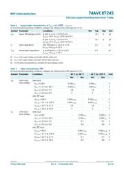
7. Limiting values
Table 2. Pin description
Symbol Pin Description
V
CC(A)
1 supply voltage A (An, OE and DIR inputs are referenced to V
CC(A)
)
DIR 2 direction control
A1 to A8 3, 4, 5, 6, 7, 8, 9, 10 data input or output
GND
[1]
11 ground (0 V)
GND
[1]
12 ground (0 V)
GND
[1]
13 ground (0 V)
B1 to B8 21, 20, 19, 18, 17, 16, 15, 14 data input or output
OE
22 output enable input (active LOW)
V
CC(B)
23 supply voltage B (Bn inputs are referenced to V
CC(B)
)
V
CC(B)
24 supply voltage B (Bn inputs are referenced to V
CC(B)
)
Table 3. Function table
[1]
Supply voltage Input Input/output
[3]
V
CC(A)
, V
CC(B)
OE
[2]
DIR
[2]
An
[2]
Bn
0.8 V to 3.6 V L L An = Bn input
0.8 V to 3.6 V L H input Bn = An
0.8 V to 3.6 V H X Z Z
GND
[3]
XXZZ
Table 4. Limiting values
In accordance with the Absolute Maximum Rating System (IEC 60134). Voltages are referenced to GND (ground = 0 V).
Symbol Parameter Conditions Min Max Unit
V
CC(A)
supply voltage A 0.5 +4.6 V
V
CC(B)
supply voltage B 0.5 +4.6 V
I
IK
input clamping current V
I
<0V 50 - mA
V
I
input voltage
[1]
0.5 +4.6 V
I
OK
output clamping current V
O
<0V 50 - mA
V
O
output voltage Active mode
[1][2][3]
0.5 V
CCO
+0.5 V
Suspend or 3-state mode
[1]
0.5 +4.6 V
I
O
output current V
O
=0VtoV
CC
- 50 mA
I
CC
supply current per V
CC(A)
or V
CC(B)
pin - 100 mA
器件 Datasheet 文档搜索
AiEMA 数据库涵盖高达 72,405,303 个元件的数据手册,每天更新 5,000 多个 PDF 文件
