Datasheet 搜索 > DA转换器 > ADI(亚德诺) > AD5331BRU-REEL7 数据手册 > AD5331BRU-REEL7 数据手册 11/28 页


¥ 0
AD5331BRU-REEL7 数据手册 - ADI(亚德诺)
制造商:
ADI(亚德诺)
分类:
DA转换器
封装:
TSSOP
描述:
2.5 V至5.5 V , 115 μA ,并行接口单电压输出8位/ 10位/ 12位DAC 2.5 V to 5.5 V, 115 μA, Parallel Interface Single Voltage-Output 8-/10-/12-Bit DACs
Pictures:
3D模型
符号图
焊盘图
引脚图
产品图
页面导航:
引脚图在P7P8P9P10P23Hot
典型应用电路图在P21
原理图在P1P7P8P9P10
封装尺寸在P24
型号编码规则在P25
焊接温度在P6
功能描述在P1P7P8P9P10
技术参数、封装参数在P1P3P6
应用领域在P1P21
电气规格在P13
导航目录
AD5331BRU-REEL7数据手册
Page:
of 28 Go
若手册格式错乱,请下载阅览PDF原文件
AD5330/AD5331/AD5340/AD5341
Rev. A | Page 11 of 28
TERMINOLOGY
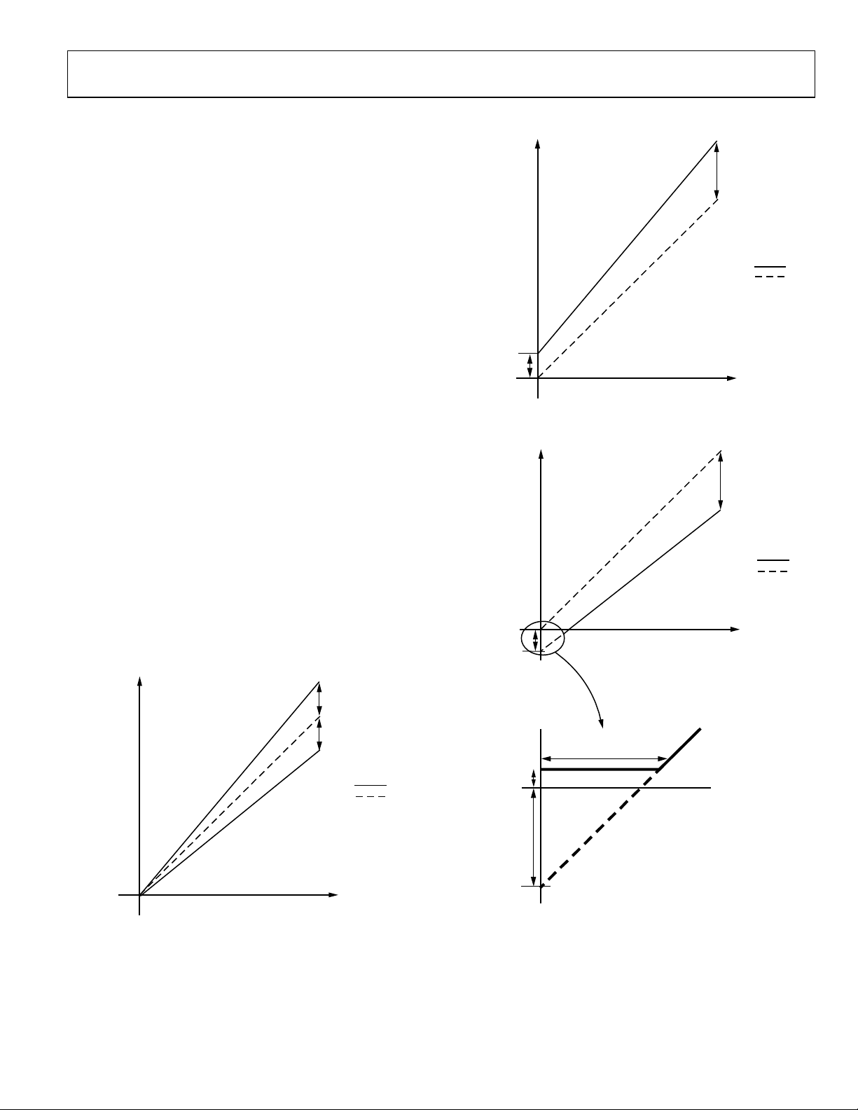
OUTPUT
VOLTAGE
DAC CODE
POSITIVE
OFFSET
GAIN ERROR
AND
OFFSET ERROR
ACTUAL
IDEAL
06852-012
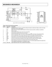
Relative Accuracy or Integral Nonlinearity (INL)
For the DAC, relative accuracy or INL is a measure of the
maximum deviation, in LSBs, from a straight line passing
through the actual endpoints of the DAC transfer function.
Typical INL vs. code plots can be seen in Figure 14, Figure 15,
and Figure 16.
Differential Nonlinearity (DNL)
DNL is the difference between the measured change and the
ideal 1 LSB change between any two adjacent codes. A specified
differential nonlinearity of ±1 LSB maximum ensures mono-
tonicity. This DAC is guaranteed monotonic by design. Typical
DNL vs. code plots can be seen in Figure 17, Figure 18, and
Figure 19.
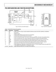
Gain Error
This is a measure of the span error of the DAC (including any
error in the gain of the buffer amplifier). It is the deviation in
slope of the actual DAC transfer characteristic from the ideal,
expressed as a percentage of the full-scale range. This is
illustrated in Figure 11.
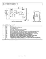
Figure 12. Positive Offset Error and Gain Error
OUTPUT
VOLTAGE
DAC CODE
NEGATIVE
OFFSET
GAIN ERROR
AND
OFFSET ERROR
ACTUAL
IDEAL
AMPLIFIER
FOOTROOM
(~1mV)
NEGATIVE
OFFSET
DEADBAND CODES
0
6852-013
Offset Error
This is a measure of the offset error of the DAC and the output
amplifier. It is expressed as a percentage of the full-scale range.
If the offset voltage is positive, the output voltage is still positive
at zero input code. This is shown in Figure 12. Because the
DACs operate from a single supply, a negative offset cannot
appear at the output of the buffer amplifier. Instead, there is
a code close to zero at which the amplifier output saturates
(amplifier footroom). Below this code, there is a deadband over
which the output voltage does not change. This is illustrated in
Figure 13.
OUTPUT
V
OLTAGE
DAC CODE
POSITIVE
GAIN ERROR
ACTUAL
IDEAL
NEGATIVE
GAIN ERROR
06852-011
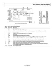
Figure 13. Negative Offset Error and Gain Error
Figure 11. Gain Error
器件 Datasheet 文档搜索
AiEMA 数据库涵盖高达 72,405,303 个元件的数据手册,每天更新 5,000 多个 PDF 文件
