Datasheet 搜索 > DA转换器 > ADI(亚德诺) > AD7302BRU-REEL 数据手册 > AD7302BRU-REEL 数据手册 3/16 页


¥ 31.549
AD7302BRU-REEL 数据手册 - ADI(亚德诺)
制造商:
ADI(亚德诺)
分类:
DA转换器
封装:
TSSOP
Pictures:
3D模型
符号图
焊盘图
引脚图
产品图
页面导航:
导航目录
AD7302BRU-REEL数据手册
Page:
of 16 Go
若手册格式错乱,请下载阅览PDF原文件
AD7302
–3–
REV. 0
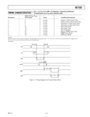
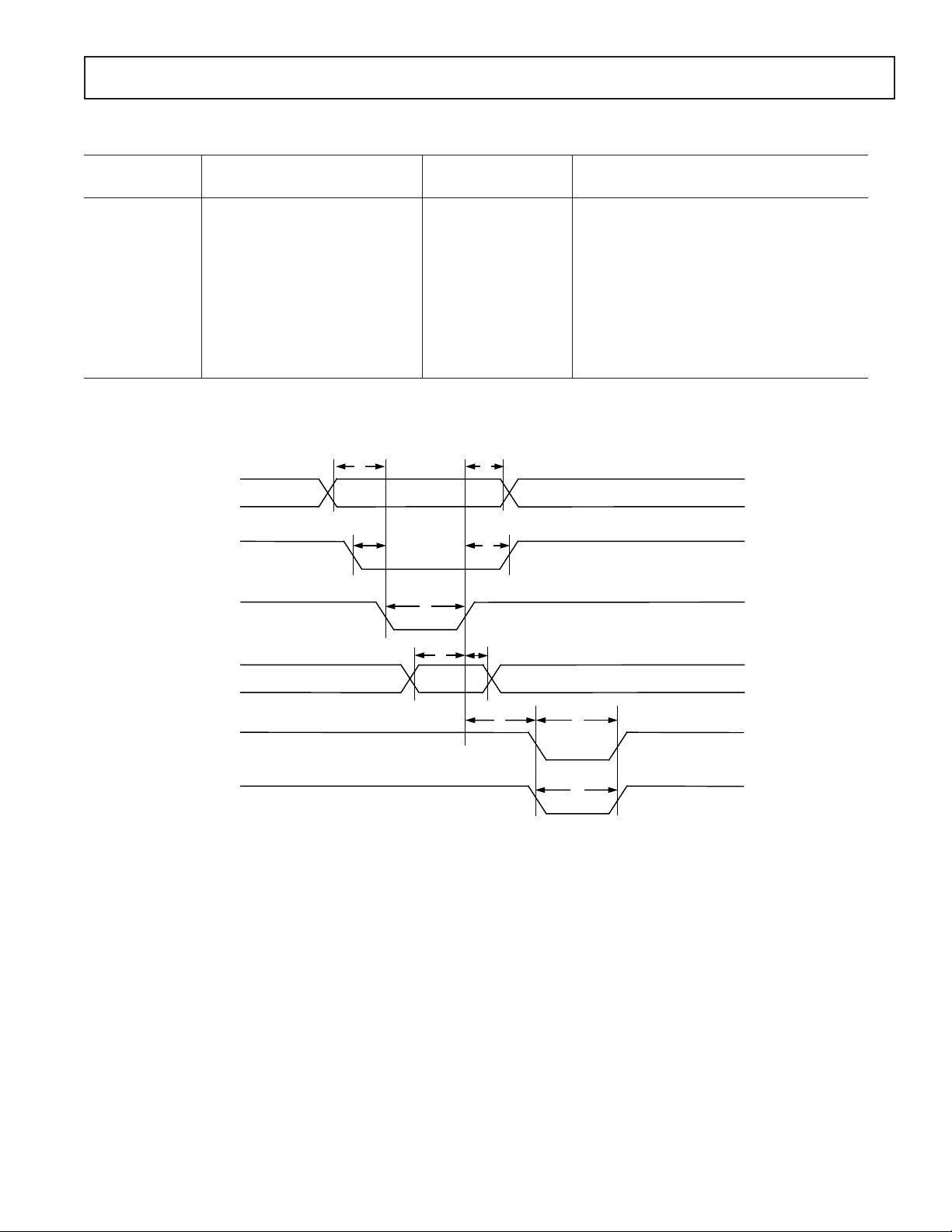
TIMING CHARACTERISTICS
1, 2
Limit at T
MIN
, T
MAX
Parameter (B Version) Units Conditions/Comments
t
1
0 ns min Address to Write Setup Time
t
2
0 ns min Address Valid to Write Hold Time
t
3
0 ns min Chip Select to Write Setup Time
t
4
0 ns min Chip Select to Write Hold Time
t
5
20 ns min Write Pulse Width
t
6
15 ns min Data Setup Time
t
7
4.5 ns min Data Hold Time
t
8
20 ns min Write to LDAC Setup Time
t
9
20 ns min LDAC Pulse Width
t
10
20 ns min CLR Pulse Width
NOTES
1
Sample tested at +25°C to ensure compliance. All input signals are specified with tr = tf = 5 ns (10% to 90% of V
DD
) and timed from a voltage level of
(V
IL
+ V
IH
)/2. tr and tf should not exceed 1 µs on any digital input.
2
See Figure 1.
A/B
CS
WR
D7–D0
LDAC
CLR
t
1
t
2
t
4
t
3
t
5
t
6
t
7
t
8
t
10
t
9
Figure 1. Timing Diagram for Parallel Data Write
(V
DD
= +2.7 V to +5.5 V; GND = 0 V; Reference = Internal V
DD
/2 Reference;
all specifications T
MIN
to T
MAX
unless otherwise noted)
器件 Datasheet 文档搜索
AiEMA 数据库涵盖高达 72,405,303 个元件的数据手册,每天更新 5,000 多个 PDF 文件
