Datasheet 搜索 > AD转换器 > ADI(亚德诺) > AD7891BSZ-2 数据手册 > AD7891BSZ-2 数据手册 16/20 页
 器件3D模型
¥ 107.335
AD7891BSZ-2 数据手册 - ADI(亚德诺)
制造商:
ADI(亚德诺)
分类:
AD转换器
封装:
QFP-44
描述:
ANALOG DEVICES AD7891BSZ-2 模数转换器, 12 bit, 500 kSPS, 单, 5 V, MQFP
Pictures:
3D模型
符号图
焊盘图
引脚图
产品图
页面导航:
导航目录
AD7891BSZ-2数据手册
Page:
of 20 Go
若手册格式错乱,请下载阅览PDF原文件
AD7891
–16–
REV. D
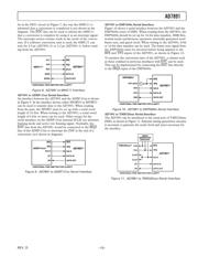
PARALLEL INTERFACING
The parallel port on the AD7891 allows the device to be interfaced
to microprocessors or DSP processors as a memory mapped
or I/O mapped device. The CS and RD inputs are common to
all memory peripheral interfacing. Typical interfaces to different
processors are shown in Figures 12 to 15. In all the interfaces
shown, an external timer controls the CONVST input of the
AD7891 and the EOC output interrupts the host DSP.
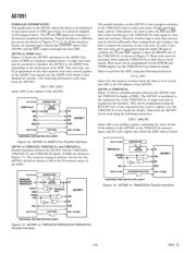
AD7891 to ADSP-21xx
Figure 12 shows the AD7891 interfaced to the ADSP-21xx
series of DSPs as a memory mapped device. A single wait state
may be necessary to interface the AD7891 to the ADSP-21xx
depending on the clock speed of the DSP. This wait state can
be programmed via the data memory wait state control register
of the ADSP-21xx (please see the ADSP-2100 family Users
Manual for details). The following instruction reads data
from the AD7891.
MR = DM (ADC)
where ADC is the address of the AD7891.
DATA BUS
ADDRESS BUS
DB11 TO DB0
AD7891*
*ADDITIONAL PINS OMITTED FOR CLARITY
CS
WR
IRQ2
D23 TO D8
EOC
RD
WR
RD
ADDR
DECODE
EN
DMS
ADSP-21xx*
A13 TO A0
Figure 12. AD7891 to ADSP-21xx Parallel Interface
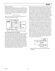
AD7891 to TMS32020, TMS320C25, and TMS320C5x
Parallel interfaces between the AD7891 and the TMS32020,
TMS320C25, and TMS320C5x family of DSPs are shown in
Figure 13. The memory mapped address chosen for the
AD7891 should be chosen to fall in the I/O memory space of
the DSPs.
TMS320C25
ONLY
DATA BUS
ADDRESS BUS
DB11 TO DB0
AD7891*
*ADDITIONAL PINS OMITTED FOR CLARITY
CS
WR
INTx
D23 TO D0
EOC
RD
MSC
ADDR
DECODE
EN
IS
A15 TO A0
TMS32020/
TMS320C25/
TMS320C5x*
READY
R/W
STRB
Figure 13. AD7891 to TMS32020/TMS320C25/TMS320C5x
Parallel Interface
The parallel interface on the AD7891 is fast enough to interface
to the TMS32020 with no extra wait states. If high speed glue
logic, such as 74AS devices, are used to drive the WR and RD
lines when interfacing to the TMS320C25, then again no wait
states are necessary. However, if slower logic is used, data accesses
may be slowed sufficiently when reading from and writing to the
part to require the insertion of one wait state. In such a case,
this wait state can be generated using the single OR gate to
combine the CS and MSC signals to drive the READY line of
the TMS320C25, as shown in Figure 13. Extra wait states are
necessary when using the TMS320C5x at their fastest clock
speeds. Wait states can be programmed via the IOWSR and
CWSR registers (see the TMS320C5x User Guide for details).
Data is read from the ADC using the following instruction:
IN D, ADC
where D is the memory location where the data is to be stored,
and ADC is the I/O address of the AD7891.
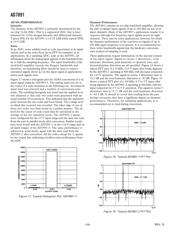
AD7891 to TMS320C3x
Figure 14 shows a parallel interface between the AD7891 and
the TMS320C3x family of DSPs. The AD7891 is interfaced to
the expansion bus of the TMS320C3x. A single wait state is
required in this interface. This can be programmed using the
WTCNT bits of the expansion bus control register (see the
TMS320C3x Users Guide for details). Data from the AD7891
can be read using the following instruction:
LDI ARn Rx¥ ,
where ARn is an auxiliary register containing the lower 16 bits
of the address of the AD7891 in the TMS320C3x memory
space, and Rx is the register into which the ADC data is loaded.
EXPANSION DATA BUS
ADDRESS BUS
DB11 TO DB0
AD7891*
*ADDITIONAL PINS OMITTED FOR CLARITY
CS
WR
INTx
XD23 TO XD0
EOC
RD
ADDR
DECODE
XA15 TO XA0
XR/W
IOSTRB
TMS320C3x*
Figure 14. AD7891 to TMS320C3x Parallel Interface
器件 Datasheet 文档搜索
AiEMA 数据库涵盖高达 72,405,303 个元件的数据手册,每天更新 5,000 多个 PDF 文件
