Datasheet 搜索 > AD转换器 > ADI(亚德诺) > AD7891BSZ-2 数据手册 > AD7891BSZ-2 数据手册 17/20 页
 器件3D模型
¥ 107.335
AD7891BSZ-2 数据手册 - ADI(亚德诺)
制造商:
ADI(亚德诺)
分类:
AD转换器
封装:
QFP-44
描述:
ANALOG DEVICES AD7891BSZ-2 模数转换器, 12 bit, 500 kSPS, 单, 5 V, MQFP
Pictures:
3D模型
符号图
焊盘图
引脚图
产品图
页面导航:
导航目录
AD7891BSZ-2数据手册
Page:
of 20 Go
若手册格式错乱,请下载阅览PDF原文件
AD7891
–17–
REV. D
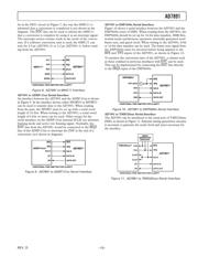
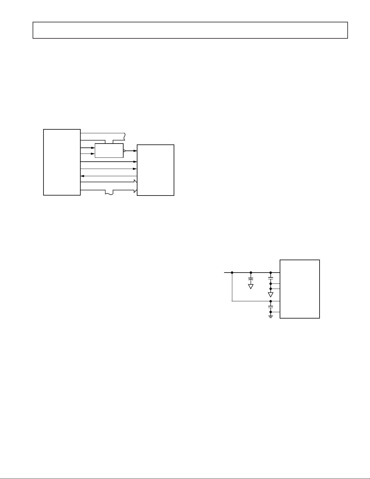
AD7891 to DSP5600x
Figure 15 shows a parallel interface between the AD7891 and
the DSP5600x series of DSPs. The AD7891 should be mapped
into the top 64 locations of Y data memory. If extra wait states
are needed in this interface, they can be programmed using the
Port A Bus control register (see the DSP5600x Users Manual
for details). Data can be read from the AD7891 using the fol-
lowing instruction:
MOVEO Y: ADC, X0
where ADC is the address in the DSP5600x address space to
which the AD7891 has been mapped.
DATA BUS
ADDRESS BUS
DB11 TO DB0
AD7891*
*ADDITIONAL PINS OMITTED FOR CLARITY
CS
WR
IRQ
D23 TO D0
EOC
RD
WR
RD
ADDR
DECODE
DS
A15 TO A0
X/Y
DSP56000/
DSP56002*
Figure 15. AD7891 to DSP5600x Parallel Interface
Power Supply Bypassing and Grounding
In any circuit where accuracy is important, careful consideration
of the power supply and ground return layout helps to ensure
the specified performance. The PCB on which the AD7891 is
mounted should be designed such that the analog and digital
sections are separated and confined to certain areas of the board.
This facilitates the use of ground planes that can be separated
easily. A minimum etch technique is generally best for ground
planes because it gives the best shielding. Digital and analog
ground planes should be joined at only one place. If the AD7891
is the only device requiring an AGND to DGND connection,
then the ground planes should be connected at the AGND and
DGND pins of the AD7891. If the AD7891 is in a system where
multiple devices require an AGND to DGND connection, the
connection should still be made at one point only, a star ground
point established as close as possible to the AD7891.
Digital lines running under the device should be avoided because
these couple noise onto the die. The analog ground plane should
be allowed to run under the AD7891 to avoid noise coupling.
The power supply lines of the AD7891 should use as large a
trace as possible to provide low impedance paths and reduce the
effects of glitches on the power supply line. Fast switching sig-
nals like clocks should be shielded with digital ground to avoid
radiating noise to other parts of the board and should never be
run near the analog inputs. Avoid crossover of digital and analog
signals. Traces on opposite sides of the board should run at right
angles to each other. This reduces the effects of feedthrough
through the board. A microstrip technique is by far the best
technique but is not always possible with a double-sided board.
In this technique, the component side of the board is dedicated
to ground plane while signal traces are placed on the solder side.
The AD7891 should have ample supply bypassing located as close
to the package as possible, ideally right up against the device.
One of the V
DD
pins (Pin 10 of the PLCC package and Pin 4
on the MQFP package) mainly drives the analog circuitry on
the chip. This pin should be decoupled to the analog ground
plane with a 10 mF tantalum bead capacitor in parallel with a
0.1 mF capacitor. The other V
DD
pin (Pin 19 on the PLCC
package and Pin 13 on the MQFP package) mainly drives
digital circuitry on the chip. This pin should be decoupled to the
digital ground plane with a 0.1 mF capacitor. The 0.1 mF
capacitors should have low effective series resistance (ESR) and
effective series inductance (ESI), such as the common ceramic
types or surface mount types, which provide a low impedance
path to ground at high frequencies to handle transient currents
due to internal logic switching. Figure 16 shows the
recommended decoupling scheme.
V
DD
(PIN 10, PLCC
PIN 4, MQFP)
DGND
AD7891
AGND
AGND
V
DD
(PIN 19, PLCC
PIN 13, MQFP)
10F
0.1F
0.1F
Figure 16. Recommended Decoupling Scheme for
the AD7891
器件 Datasheet 文档搜索
AiEMA 数据库涵盖高达 72,405,303 个元件的数据手册,每天更新 5,000 多个 PDF 文件
