Datasheet 搜索 > DA转换器 > ADI(亚德诺) > AD7948BRSZ 数据手册 > AD7948BRSZ 数据手册 4/16 页
 器件3D模型
¥ 1.449
AD7948BRSZ 数据手册 - ADI(亚德诺)
制造商:
ADI(亚德诺)
分类:
DA转换器
封装:
SSOP-20
描述:
ANALOG DEVICES AD7948BRSZ 数模转换器, 12 bit, 17 MSPS, 串行, 3V 至 5.5V, 4.5V 至 5.5V, SSOP, 20 引脚
Pictures:
3D模型
符号图
焊盘图
引脚图
产品图
页面导航:
导航目录
AD7948BRSZ数据手册
Page:
of 16 Go
若手册格式错乱,请下载阅览PDF原文件
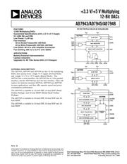
AD7943/AD7945/AD7948
REV. B–4–
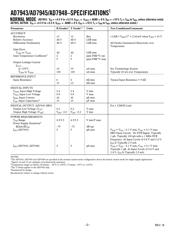
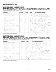
AC PERFORMANCE CHARACTERISTICS
NORMAL MODE
Parameter B Grades T Grade Units Test Conditions/Comments
DYNAMIC PERFORMANCE
Output Voltage Settling Time 600 700 ns typ To 0.01% of Full-Scale Range. V
REF
=
+10 V; DAC Latch Alternately Loaded with
All 0s and All 1s
Digital to Analog Glitch Impulse 60 60 nV-s typ Measured with V
REF
= 0 V. DAC Latch
Alternately Loaded with All 0s and All 1s
Multiplying Feedthrough Error –75 –75 dB max DAC Latch Loaded with All 0s
Output Capacitance 60 60 pF max All 1s Loaded to DAC
30 30 pF max All 0s Loaded to DAC
Digital Feedthrough (AD7943) 5 5 nV-s typ Feedthrough to the DAC Output with LD1,
LD2 High and Alternate Loading of All 0s
and All 1s into the Input Shift Register
Digital Feedthrough (AD7945, AD7948) 5 5 nV-s typ Feedthrough to the DAC Output with CS
High and Alternate Loading of All 0s and
All 1s to the DAC Bus
Total Harmonic Distortion –83 –83 dB typ
Output Noise Spectral Density
@ 1 kHz 35 35 nV/√Hz typ All 1s Loaded to DAC. V
REF
= 0 V. Output
Op Amp Is OP07
Specifications subject to change without notice.
(AD7943: V
DD
= +4.5 V to +5.5 V; V
IOUT1
= V
IOUT2
= AGND = 0 V. AD7945, AD7948: V
DD
= +4.5 V to +5.5 V; V
IOUT1
=AGND =
0 V. V
REF
= 6 V rms, 1 kHz sine wave; T
A
= T
MIN
to T
MAX
; DAC output op amp is AD843; unless otherwise noted.) These characteristics are in-
cluded for Design Guidance and are not subject to test.
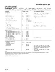
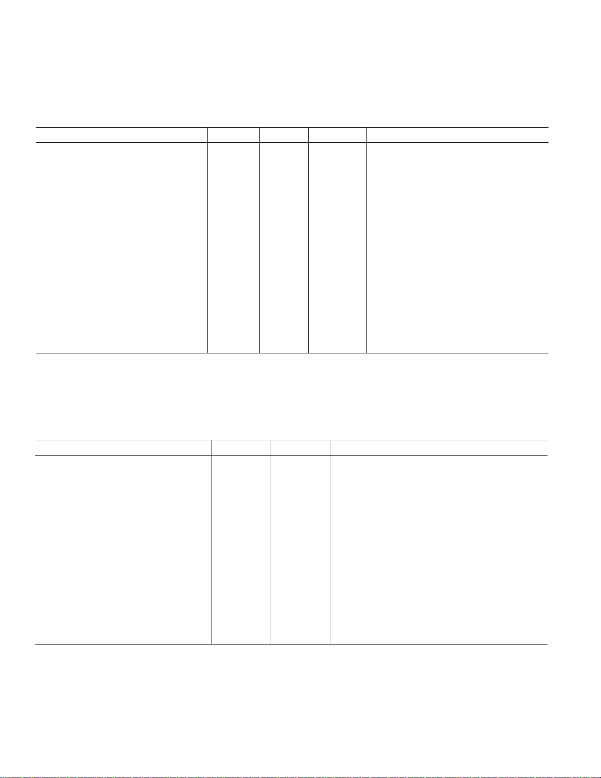
AC PERFORMANCE CHARACTERISTICS
BIASED MODE
(AD7943: V
DD
= +3 V to +5.5 V; V
IOUT1
= V
IOUT2
= AGND = 1.23 V. AD7945, AD7948: V
DD
= +3 V to +5.5 V; V
IOUT1
= AGND =
1.23 V. V
REF
= 1 kHz, 2.45 V p-p, sine wave biased at 1.23 V; DAC output op amp is AD820; T
A
= T
MIN
to T
MAX
; unless otherwise noted.) These
characteristics are included for Design Guidance and are not subject to test.
Parameter A Grades Units Test Conditions/Comments
DYNAMIC PERFORMANCE
Output Voltage Settling Time 5 µs typ To 0.01% of Full-Scale Range. V
REF
= 0 V
DAC Latch Alternately Loaded with All 0s and All 1s
Digital to Analog Glitch Impulse 60 nV-s typ V
REF
= 1.23 V. DAC Register Alternately Loaded
with All 0s and All 1s
Multiplying Feedthrough Error –75 dB max DAC Latch Loaded with All 0s
Output Capacitance 60 pF max All 1s Loaded to DAC
30 pF max All 0s Loaded to DAC
Digital Feedthrough 5 nV-s typ Feedthrough to the DAC Output with LD1, LD2
High and Alternate Loading of All 0s and All 1s
into the Input Shift Register
Digital Feedthrough (AD7945, AD7948) 5 nV-s typ Feedthrough to the DAC Output with CS High
and Alternate Loading of All 0s and All 1s to the
DAC Bus
Total Harmonic Distortion –83 dB typ
Output Noise Spectral Density
@ 1 kHz 25 nV/√Hz typ All 1s Loaded to DAC. V
REF
= 1.23 V
Specifications subject to change without notice.
器件 Datasheet 文档搜索
AiEMA 数据库涵盖高达 72,405,303 个元件的数据手册,每天更新 5,000 多个 PDF 文件
