Datasheet 搜索 > DA转换器 > ADI(亚德诺) > AD7948BRSZ 数据手册 > AD7948BRSZ 数据手册 5/16 页
 器件3D模型
¥ 1.449
AD7948BRSZ 数据手册 - ADI(亚德诺)
制造商:
ADI(亚德诺)
分类:
DA转换器
封装:
SSOP-20
描述:
ANALOG DEVICES AD7948BRSZ 数模转换器, 12 bit, 17 MSPS, 串行, 3V 至 5.5V, 4.5V 至 5.5V, SSOP, 20 引脚
Pictures:
3D模型
符号图
焊盘图
引脚图
产品图
页面导航:
导航目录
AD7948BRSZ数据手册
Page:
of 16 Go
若手册格式错乱,请下载阅览PDF原文件
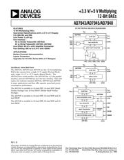
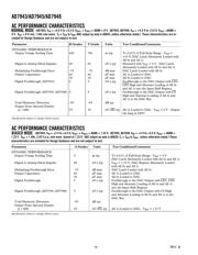
AD7943/AD7945/AD7948
REV. B –5–
(T
A
= T
MIN
to T
MAX
, unless otherwise noted)
Limit @ Limit @
Parameter V
DD
= +3 V to +3.6 V V
DD
= +4.5 V to +5.5 V Units Description
t
STB
2
60 40 ns min STB Pulsewidth
t
DS
15 10 ns min Data Setup Time
t
DH
35 25 ns min Data Hold Time
t
SRI
55 35 ns min SRI Data Pulsewidth
t
LD
55 35 ns min Load Pulsewidth
t
CLR
55 35 ns min CLR Pulsewidth
t
ASB
0 0 ns min Min Time Between Strobing Input Shift
Register and Loading DAC Register
t
SV
3
60 35 ns max STB Clocking Edge to SRO Data Valid Delay
NOTES
1
All input signals are specified with tr = tf = 5 ns (10% to 90% of 5 V) and timed from a voltage level of 1.6 V. tr and tf should not exceed 1 µs on any digital input.
2
STB mark/space ratio range is 60/40 to 40/60.
3
t
SV
is measured with the load circuit of Figure 2 and defined as the time required for the output to cross 0.8 V or 2.4 V.
Specifications subject to change without notice.
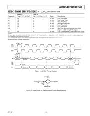
t
STB
STB1,
STB2,
STB4
STB3
t
DS
t
DH
t
SRI
SRI
DB11(N)
(MSB)
DB10(N)
DB0(N)
DB0(N–1)
DB10(N–1)
LD1,
LD2,
CLR
SRO
t
SV
t
LD
, t
CLR
t
ASB
Figure 1. AD7943 Timing Diagram
TO OUTPUT
PIN
C
L
50pF
1.6mA
I
OL
+2.1V
I
OH
200mA
Figure 2. Load Circuit for Digital Output Timing Specifications
AD7943 TIMING SPECIFICATIONS
1
器件 Datasheet 文档搜索
AiEMA 数据库涵盖高达 72,405,303 个元件的数据手册,每天更新 5,000 多个 PDF 文件
