Datasheet 搜索 > 稳压芯片 > ADI(亚德诺) > ADP7112ACBZ-1.2-R7 数据手册 > ADP7112ACBZ-1.2-R7 数据手册 14/22 页
 器件3D模型
¥ 7.511
ADP7112ACBZ-1.2-R7 数据手册 - ADI(亚德诺)
制造商:
ADI(亚德诺)
分类:
稳压芯片
封装:
WLCSP-6
描述:
20 V、200, m, A低噪声CMOS LDO线性稳压器
Pictures:
3D模型
符号图
焊盘图
引脚图
产品图
页面导航:
导航目录
ADP7112ACBZ-1.2-R7数据手册
Page:
of 22 Go
若手册格式错乱,请下载阅览PDF原文件
Data Sheet ADP7112
Rev. C | Page 13 of 21
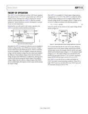
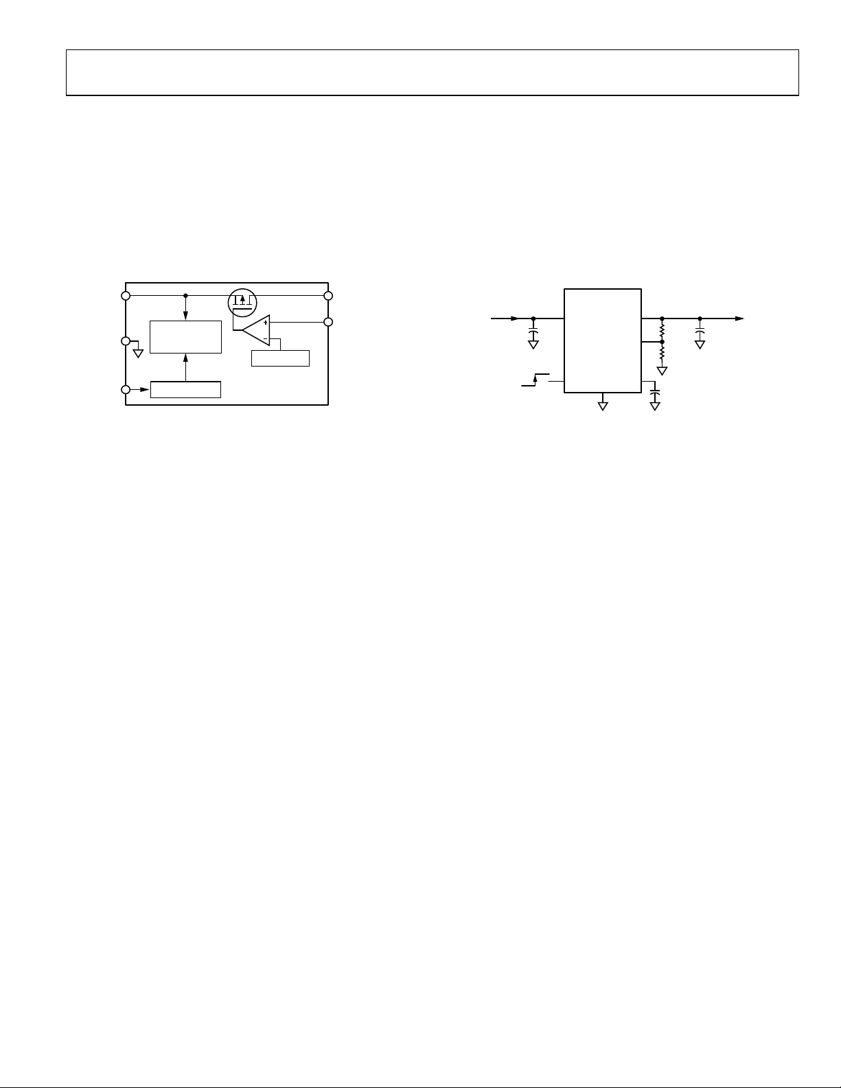
THEORY OF OPERATION
The ADP7112 is a low quiescent current, LDO linear regulator
that operates from 2.7 V to 20 V and provides up to 200 mA of
output current. Drawing a low 180 μA of quiescent current
(typical) at full load makes the ADP7112 ideal for portable
equipment. Typical shutdown current consumption is around
3.0 μA at room temperature.
Optimized for use with small 2.2 µF ceramic capacitors, the
ADP7112 provides excellent transient performance.
VOUT
SENSE/
ADJ
GND
SHORT-CIRCUIT,
THERMAL
PROTECTION
REFERENCE
SHUTDOWN
EN
VIN
12508-040
Figure 40. Internal Block Diagram
Internally, the ADP7112 consists of a reference, an error amplifier, a
feedback voltage divider, and a PMOS pass transistor. Output
current is delivered via the PMOS pass device, which is controlled
by the error amplifier. The error amplifier compares the reference
voltage with the feedback voltage from the output and amplifies
the difference. If the feedback voltage is lower than the reference
voltage, the gate of the PMOS device is pulled lower, allowing more
current to pass and increasing the output voltage. If the feedback
voltage is higher than the reference voltage, the gate of the PMOS
device is pulled higher, allowing less current to pass and decreasing
the output voltage.
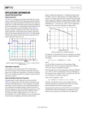
The ADP7112 is available in 15 fixed output voltage options,
ranging from 1.2 V to 5.0 V. The ADP7112 architecture allows
any fixed output voltage to be set to a higher voltage with an
external voltage divider. For example, a fixed 5 V output can be
set to a 6 V output according to the following equation:
V
OUT
= 5 V(1 + R1/R2) (3)
where R1 and R2 are the resistors in the output voltage divider
shown in Figure 41.
VOUT
SENSE/ADJ
VIN
ADP7112
GND
SS
C
SS
1nF
C
IN
2.2µF
C
OUT
2.2µF
EN
OFF
ON
V
IN
= 7V V
OUT
= 6V
R1
2kΩ
R2
10kΩ
12508-041
Figure 41. Typical Adjustable Output Voltage Application Schematic
It is recommended that the R2 value be less than 200 kΩ to
minimize errors in the output voltage caused by the SENSE/
ADJ pin input current. For example, when R1 and R2 each equal
200 kΩ and the default output voltage is 1.2 V, the adjusted output
voltage is 2.4 V. The output voltage error introduced by the
SENSE/ADJ pin input current is 1 mV or 0.04%, assuming a
typical SENSE/ADJ pin input current of 10 nA at 25°C.
The ADP7112 uses the EN pin to enable and disable the
VOUT pin under normal operating conditions. When EN is
high, VOUT turns on, and when EN is low, VOUT turns off.
For automatic startup, tie EN to VIN.
器件 Datasheet 文档搜索
AiEMA 数据库涵盖高达 72,405,303 个元件的数据手册,每天更新 5,000 多个 PDF 文件
