Datasheet 搜索 > 稳压芯片 > ADI(亚德诺) > ADP7112ACBZ-1.2-R7 数据手册 > ADP7112ACBZ-1.2-R7 数据手册 15/22 页
 器件3D模型
¥ 7.563
ADP7112ACBZ-1.2-R7 数据手册 - ADI(亚德诺)
制造商:
ADI(亚德诺)
分类:
稳压芯片
封装:
WLCSP-6
描述:
20 V、200, m, A低噪声CMOS LDO线性稳压器
Pictures:
3D模型
符号图
焊盘图
引脚图
产品图
页面导航:
导航目录
ADP7112ACBZ-1.2-R7数据手册
Page:
of 22 Go
若手册格式错乱,请下载阅览PDF原文件
ADP7112 Data Sheet
Rev. C | Page 14 of 21
APPLICATIONS INFORMATION
CAPACITOR SELECTION
Output Capacitor
The ADP7112 is designed for operation with small, space-saving
ceramic capacitors, but functions with general-purpose capacitors
as long as care is taken with regard to the effective series resistance
(ESR) value. The ESR of the output capacitor affects the stability of
the LDO control loop. A 2.2 µF capacitance with an ESR of 0.3 Ω or
less is recommended to ensure the stability of the ADP7112.
Transie nt response to changes in load current is also affected by
output capacitance. Using a larger value of output capacitance
improves the transient response of the ADP7112 to large changes
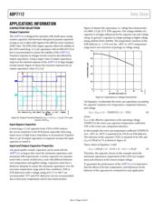
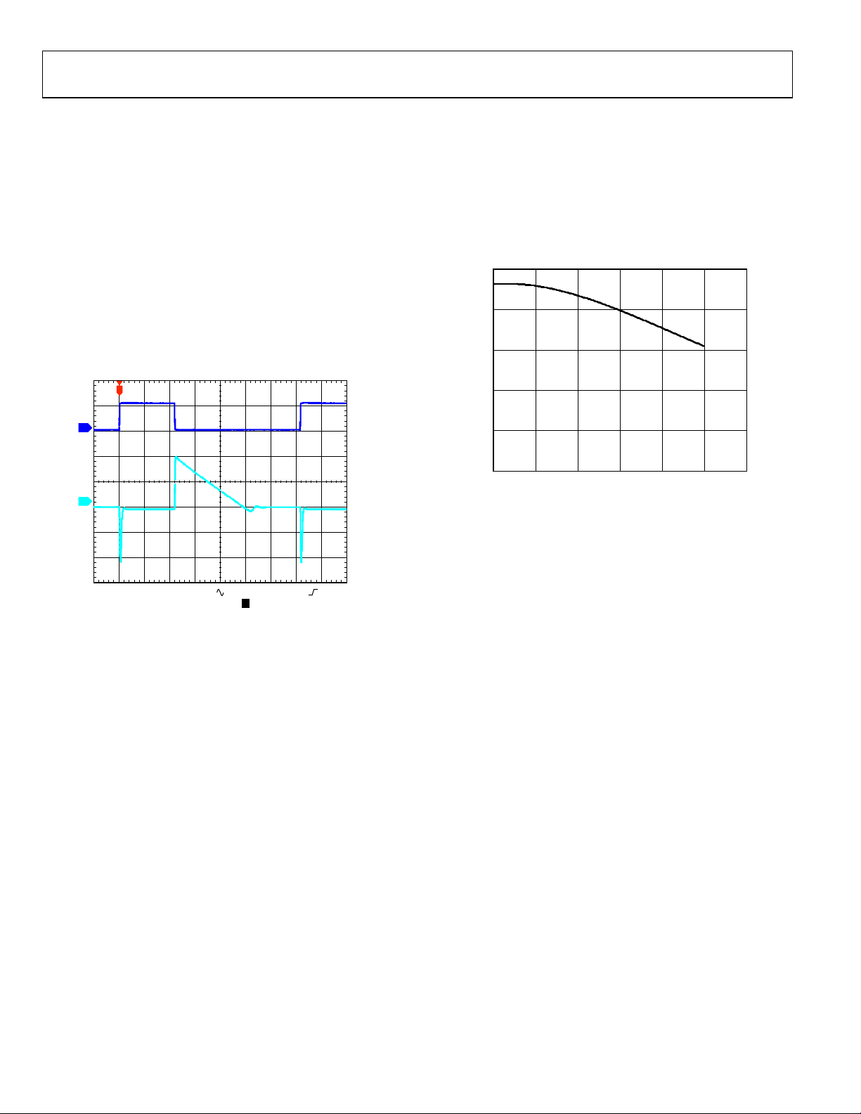
in load current. Figure 42 shows the transient responses for an
output capacitance value of 2.2 µF.
CH1 200mA Ω
B
W
M20µs A CH1 100mA
T 10.2%
1
2
CH2 20mV
B
W
T
12508-042
Figure 42. Output Transient Response, V
OUT
= 5 V, C
OUT
= 2.2 µF, CH1 Load
Current, CH2 V
OUT
Input Bypass Capacitor
Connecting a 2.2 µF capacitor from VIN to GND reduces
the circuit sensitivity to the PCB layout, especially when long
input traces or high source impedance is encountered. If greater
than 2.2 µF of output capacitance is required, increase the input
capacitor to match it.
Input and Output Capacitor Properties
Any good quality ceramic capacitors can be used with the
ADP7112, as long as they meet the minimum capacitance and
maximum ESR requirements. Ceramic capacitors are manufac-
tured with a variety of dielectrics, each with different behavior
over temperature and applied voltage. Capacitors must have a
dielectric adequate to ensure the minimum capacitance over the
necessary temperature range and dc bias conditions. X5R or
X7R dielectrics with a voltage rating of 6.3 V to 100 V are
recommended. Y5V and Z5U dielectrics are not recommended,
due to their poor temperature and dc bias characteristics.
Figure 43 depicts the capacitance vs. voltage bias characteristic
of a 0805, 2.2 µF, 10 V, X5R capacitor. The voltage stability of a
capacitor is strongly influenced by the capacitor size and voltage
rating. In general, a capacitor in a larger package or higher voltage
rating exhibits better stability. The temperature variation of the
X5R dielectric is ~±15% over the −40°C to +85°C temperature
range and is not a function of package or voltage rating.
CAPACITANCE (µF)
DC BIAS VOLTAGE (V)
121086420
0
0.5
1.0
1.5
2.0
2.5
12508-043
Figure 43. Capacitance vs. Voltage Characteristic
Use Equation 1 to determine the worst-case capacitance accounting
for capacitor variation over temperature, component tolerance,
and voltage.
C
EFF
= C
BIAS
× (1 − TEMPCO) × (1 − TOL) (4)
where:
C
BIAS
is the effective capacitance at the operating voltage.
TEMPCO is the worst-case capacitor temperature coefficient.
TOL is the worst-case component tolerance.
In this example, the worst-case temperature coefficient (TEMPCO)
over −40°C to +85°C is assumed to be 15% for an X5R dielectric.
The tolerance of the capacitor (TOL) is assumed to be 10%, and
C
BIAS
is 2.09 μF at 5 V, as shown in Figure 43.
These values in Equation 1 yield
C
EFF
= 2.09 μF × (1 − 0.15) × (1 − 0.1) = 1.59 μF (5)
Therefore, the capacitor chosen in this example meets the
minimum capacitance requirement of the LDO over temper-
ature and tolerance at the chosen output voltage.
To guarantee the performance of the ADP7112, it is imperative
that the effects of dc bias, temperature, and tolerances on the
behavior of the capacitors be evaluated for each application.
器件 Datasheet 文档搜索
AiEMA 数据库涵盖高达 72,405,303 个元件的数据手册,每天更新 5,000 多个 PDF 文件
