Datasheet 搜索 > AD转换器 > TI(德州仪器) > ADS5547IRGZRG4 数据手册 > ADS5547IRGZRG4 数据手册 3/57 页
 器件3D模型
¥ 0
ADS5547IRGZRG4 数据手册 - TI(德州仪器)
制造商:
TI(德州仪器)
分类:
AD转换器
封装:
QFN-48
描述:
14 - BIT , 210 MSPS的DDR LVDS / CMOS输出的ADC 14-BIT, 210 MSPS ADC WITH DDR LVDS/CMOS OUTPUTS
Pictures:
3D模型
符号图
焊盘图
引脚图
产品图
页面导航:
引脚图在P12P22P23P24P25Hot
封装尺寸在P50P52P53
型号编码规则在P2
标记信息在P2P50
封装信息在P2P50P51P52P53
技术参数、封装参数在P3P46P47P48
应用领域在P1P57
电气规格在P4P5P6
型号编号列表在P1
导航目录
ADS5547IRGZRG4数据手册
Page:
of 57 Go
若手册格式错乱,请下载阅览PDF原文件
www.ti.com
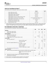
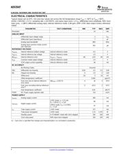
ABSOLUTE MAXIMUM RATINGS
(1)
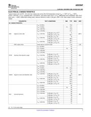
RECOMMENDED OPERATING CONDITIONS
ADS5547
SLWS192A – NOVEMBER 2006 – REVISED MAY 2007
over operating free-air temperature range (unless otherwise noted)
VALUE UNIT
Supply voltage range, AVDD –0.3 V to 3.9 V
Supply voltage range, DRVDD –0.3 V to 3.9 V
Voltage between AGND and DRGND -0.3 to 0.3 V
Voltage between AVDD to DRVDD -0.3 to 3.3 V
Voltage applied to VCM pin (in external reference mode) -0.3 to 1.8 V
Voltage applied to analog input pins, INP and INM –0.3 V to minimum (3.6, AVDD + 0.3 V) V
Voltage applied to input clock pins, CLKP and CLKM -0.3 V to AVDD + 0.3 V V
T
A
Operating free-air temperature range –40 to 85 ° C
T
J
Operating junction temperature range 125 ° C
T
stg
Storage temperature range –65 to 150 ° C
(1) Stresses beyond those listed under absolute maximum ratings may cause permanent damage to the device. These are stress ratings
only and functional operation of the device at these or any other conditions beyond those indicated under recommended operating
conditions is not implied. Exposure to absolute maximum rated conditions for extended periods may affect device reliability.
over operating free-air temperature range (unless otherwise noted)
MIN TYP MAX UNIT
SUPPLIES
Analog supply voltage, AVDD 3 3.3 3.6 V
Digital supply voltage, DRVDD 3 3.3 3.6 V
ANALOG INPUTS
Differential input voltage range 2 V
PP
Input common-mode voltage 1.5 ± 0.1 V
Voltage applied on VCM in external reference mode 1.45 1.5 1.55 V
CLOCK INPUT
Input clock sample rate
(1)
MSPS
DEFAULT SPEED mode 50 210
MSPS
LOW SPEED mode 1 60
Input clock amplitude differential (V
(CLKP)
- V
(CLKM)
)
Sine wave, ac-coupled 0.4 1.5 V
PP
LVPECL, ac-coupled 1.6 V
PP
LVDS, ac-coupled 0.7 V
PP
LVCMOS, single-ended, ac-coupled 3.3 V
Input clock duty cycle (See Figure 30 ) 35% 50% 65%
DIGITAL OUTPUTS
C
L
Maximum external load capacitance from each output pin to DRGND (LVDS and CMOS modes)
Without internal termination (default after
5 pF
reset)
With 100 Ω internal termination
(2)
10 pF
R
L
Differential load resistance between the LVDS output pairs (LVDS mode) 100 Ω
Operating free-air temperature –40 85 ° C
(1) See the section on Low Sampling Frequency Operation for more information.
(2) See the section on LVDS Buffer Internal termination for more information.
3
Submit Documentation Feedback
器件 Datasheet 文档搜索
AiEMA 数据库涵盖高达 72,405,303 个元件的数据手册,每天更新 5,000 多个 PDF 文件
