Datasheet 搜索 > AD转换器 > TI(德州仪器) > ADS5547IRGZRG4 数据手册 > ADS5547IRGZRG4 数据手册 4/57 页
 器件3D模型
¥ 0
ADS5547IRGZRG4 数据手册 - TI(德州仪器)
制造商:
TI(德州仪器)
分类:
AD转换器
封装:
QFN-48
描述:
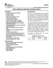
14 - BIT , 210 MSPS的DDR LVDS / CMOS输出的ADC 14-BIT, 210 MSPS ADC WITH DDR LVDS/CMOS OUTPUTS
Pictures:
3D模型
符号图
焊盘图
引脚图
产品图
页面导航:
引脚图在P12P22P23P24P25Hot
封装尺寸在P50P52P53
型号编码规则在P2
标记信息在P2P50
封装信息在P2P50P51P52P53
技术参数、封装参数在P3P46P47P48
应用领域在P1P57
电气规格在P4P5P6
型号编号列表在P1
导航目录
ADS5547IRGZRG4数据手册
Page:
of 57 Go
若手册格式错乱,请下载阅览PDF原文件
www.ti.com
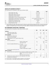
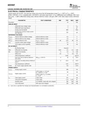
ELECTRICAL CHARACTERISTICS
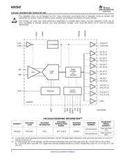
ADS5547
SLWS192A – NOVEMBER 2006 – REVISED MAY 2007
Typical values are at 25 ° C, min and max values are across the full temperature range T
MIN
= –40 ° C to T
MAX
= 85 ° C,
AVDD = DRVDD = 3.3 V, sampling rate = 210 MSPS, sine wave input clock, 1.5 V
PP
differential clock amplitude, 50% clock
duty cycle, –1 dBFS differential analog input, internal reference mode, 0 db gain, DDR LVDS data output (unless otherwise
noted)
PARAMETER TEST CONDITIONS MIN TYP MAX UNIT
Resolution 14 bits
ANALOG INPUT
Differential input voltage range 2 V
PP
Differential input capacitance 7 pF
Analog input bandwidth 800 MHz
Analog input common mode current
342 µ A
(per input pin)
REFERENCE VOLTAGES
V
(REFB)
Internal reference bottom voltage Internal reference mode 0.5 V
V
(REFT)
Internal reference top voltage Internal reference mode 2.5 V
∆ V
(REF)
Internal reference error V
(REFT)
- V
(REFB)
-60 ± 25 60 mV
V
CM
Common mode output voltage Internal reference mode 1.5 V
VCM output current capability Internal reference mode ± 4 mA
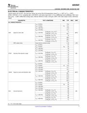
DC ACCURACY
No Missing Codes Assured
DNL Differential non-linearity -0.95 0.5 2.5 LSB
INL Integral non-linearity -5 3.5 5 LSB
Offset error -10 5 10 mV
Offset temperature coefficient 0.002 ppm/ ° C
Gain error due to internal reference ( ∆ V
(REF)
/ 2.0V) % -3 ± 1 3 %FS
error alone
Gain error excluding internal reference -2 ± 0.5 2 %FS
error
(1)
Gain temperature coefficient 0.01 ∆ %/ ° C
PSRR DC Power supply rejection ratio 0.6 mV/V
POWER SUPPLY
I
(AVDD)
Analog supply current 306 mA
LVDS mode, I
O
= 3.5 mA,
66 mA
R
L
= 100 Ω , C
L
= 5 pF
I
(DRVDD)
Digital supply current
CMOS mode, F
IN
= 2.5 MHz,
47 mA
C
L
= 5 pF
I
CC
Total supply current LVDS mode 372 mA
Total power dissipation LVDS mode 1.23 1.375 W
Standby power In STANDBY mode with clock stopped 100 150 mW
Clock stop power With input clock stopped 100 150 mW
(1) Gain error is specified from design and characterization; it is not tested in production.
4
Submit Documentation Feedback
器件 Datasheet 文档搜索
AiEMA 数据库涵盖高达 72,405,303 个元件的数据手册,每天更新 5,000 多个 PDF 文件
