Datasheet 搜索 > ON Semiconductor(安森美) > CAV24C02 数据手册 > CAV24C02 数据手册 3/15 页


¥ 0
CAV24C02 数据手册 - ON Semiconductor(安森美)
制造商:
ON Semiconductor(安森美)
描述:
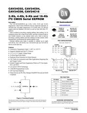
2 KB , 4 KB , 8 KB和16 KB的I2C CMOS串行EEPROM 2-Kb, 4-Kb, 8-Kb and 16-Kb I2C CMOS Serial EEPROM
Pictures:
3D模型
符号图
焊盘图
引脚图
产品图
页面导航:
引脚图在P1P5Hot
封装尺寸在P10P11P12P13
焊盘布局在P12P13
型号编码规则在P1P14P15
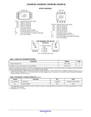
标记信息在P2P14P15
封装信息在P14
功能描述在P5
技术参数、封装参数在P2P14
应用领域在P1
电气规格在P3
型号编号列表在P2
导航目录
CAV24C02数据手册
Page:
of 15 Go
若手册格式错乱,请下载阅览PDF原文件
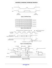
CAV24C02, CAV24C04, CAV24C08, CAV24C16
www.onsemi.com
3
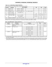
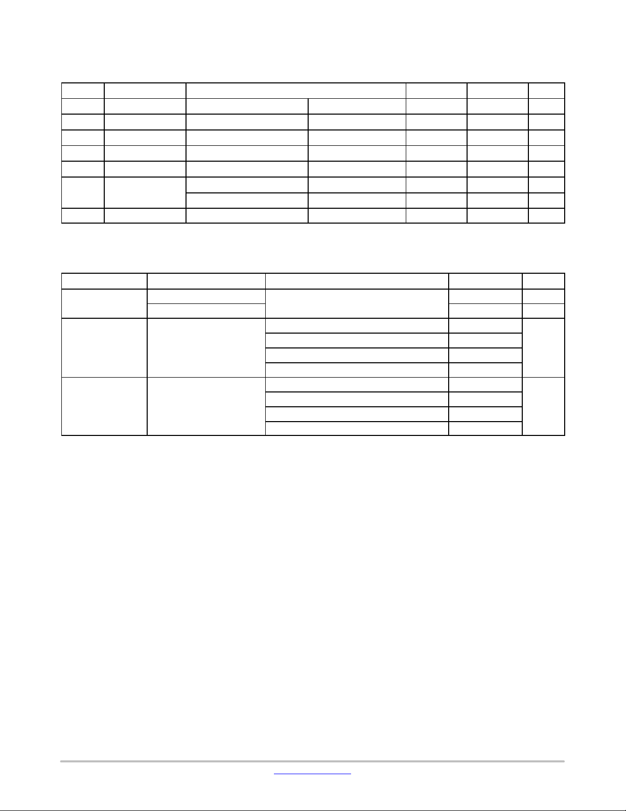
Table 3. D.C. OPERATING CHARACTERISTICS
(V
CC
= 2.5 V to 5.5 V, T
A
= −40°C to +125°C, unless otherwise specified.)
Symbol
Parameter Test Conditions Min Max Units
I
CCR
Read Current Read, f
SCL
= 400 kHz 1 mA
I
CCW
Write Current Write, f
SCL
= 400 kHz 2 mA
I
SB
Standby Current All I/O Pins at GND or V
CC
T
A
= −40°C to +125°C 5
mA
I
L
I/O Pin Leakage Pin at GND or V
CC
2
mA
V
IL
Input Low Voltage −0.5 0.3 x V
CC
V
V
IH
Input High Voltage
A
0
, A
1
, A
2
and WP 0.7 x V
CC
V
CC
+ 0.5 V
SCL and SDA 0.7 x V
CC
5.5 V
V
OL
Output Low Voltage V
CC
> 2.5 V, I
OL
= 3 mA 0.4 V
Product parametric performance is indicated in the Electrical Characteristics for the listed test conditions, unless otherwise noted. Product
performance may not be indicated by the Electrical Characteristics if operated under different conditions.
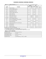
Table 4. PIN IMPEDANCE CHARACTERISTICS (V
CC
= 2.5 V to 5.5 V, T
A
= −40°C to +125°C, unless otherwise specified.)
Symbol Parameter Conditions Max Units
C
IN
(Note 4)
SDA Pin Capacitance
V
IN
= 0 V, f = 1.0 MHz, V
CC
= 5.0 V
8 pF
Other Pins 6 pF
I
WP
(Note 5) WP Input Current
V
IN
< V
IH
, V
CC
= 5.5 V 130 mA
V
IN
< V
IH
, V
CC
= 3.6 V 120
V
IN
< V
IH
, V
CC
= 2.5 V 80
V
IN
> V
IH
2
I
A
(Note 5) Address Input Current
(A0, A1, A2)
V
IN
< V
IH
, V
CC
= 5.5 V 50 mA
V
IN
< V
IH
, V
CC
= 3.6 V 35
V
IN
< V
IH
, V
CC
= 2.5 V 25
V
IN
> V
IH
2
4. These parameters are tested initially and after a design or process change that affects the parameter according to appropriate AEC−Q100
and JEDEC test methods.
5. When not driven, the WP, A0, A1 and A2 pins are pulled down to GND internally. For improved noise immunity, the internal pull−down is relatively
strong; therefore the external driver must be able to supply the pull−down current when attempting to drive the input HIGH. To conserve power,
as the input level exceeds the trip point of the CMOS input buffer (~ 0.5 x V
CC
), the strong pull−down reverts to a weak current source.
器件 Datasheet 文档搜索
AiEMA 数据库涵盖高达 72,405,303 个元件的数据手册,每天更新 5,000 多个 PDF 文件
