Datasheet 搜索 > 存储芯片 > Integrated Device Technology(艾迪悌) > IDT7006S35PF 数据手册 > IDT7006S35PF 数据手册 4/20 页
 器件3D模型
¥ 0
IDT7006S35PF 数据手册 - Integrated Device Technology(艾迪悌)
制造商:
Integrated Device Technology(艾迪悌)
分类:
存储芯片
封装:
LQFP
描述:
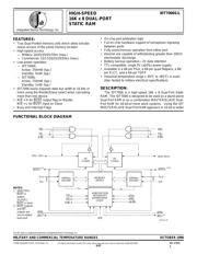
高速16K ×8双端口静态RAM HIGH-SPEED 16K x 8 DUAL-PORT STATIC RAM
Pictures:
3D模型
符号图
焊盘图
引脚图
产品图
页面导航:

导航目录
IDT7006S35PF数据手册
Page:
of 20 Go
若手册格式错乱,请下载阅览PDF原文件
6.07 4
IDT7006S/L
HIGH-SPEED 16K x 8 DUAL-PORT STATIC RAM MILITARY AND COMMERCIAL TEMPERATURE RANGES
CAPACITANCE
(1)
(TA = +25°C, f = 1.0MHz)TQFP PACKAGE
Symbol Parameter Conditions
(2)
Max. Unit
C
IN Input Capacitance VIN = 3dV 9 pF
C
OUT Output VOUT = 3dV 10 pF
Capacitance
NOTES: 2739 tbl 07
1. This parameter is determined by device characterization, but is not
production tested.
2. 3dv references the interpolated capacitance when the input and output
signals switch from 0V to 3V or from 3V to 0V.
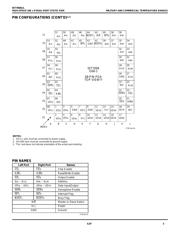
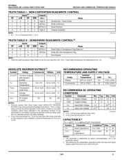
TRUTH TABLE I – NON-CONTENTION READ/WRITE CONTROL
Inputs
(1)
Outputs
CECE
CECE
CE
R/
WW
WW
W
OEOE
OEOE
OE
SEMSEM
SEMSEM
SEM
I/O
0-7 Mode
H X X H High-Z Deselected: Power-Down
L L X H DATA
IN Write to Memory
L H L H DATA
OUT Read Memory
X X H X High-Z Outputs Disabled
NOTE: 2739 tbl 02
1. A0L — A13L is not equal to A0R — A13R.
TRUTH TABLE II – SEMAPHORE READ/WRITE CONTROL
(1)
Inputs Outputs
CECE
CECE
CE
R/
WW
WW
W
OEOE
OEOE
OE
SEMSEM
SEMSEM
SEM
I/O
0-7 Mode
H H L L DATA
OUT Read Data in Semaphore Flag Data Out
H
u
X L DATA
IN Write I/O0 into Semaphore Flag
L X X L — Not Allowed
2739 tbl 03
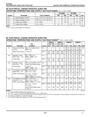
RECOMMENDED DC OPERATING
CONDITIONS
Symbol Parameter Min. Typ. Max. Unit
V
CC Supply Voltage 4.5 5.0 5.5 V
GND Supply Voltage 0 0 0 V
V
IH Input High Voltage 2.2 — 6.0
(2)
V
V
IL Input Low Voltage –0.5
(1)
— 0.8 V
NOTES: 2739 tbl 06
1. VIL≥ -1.5V for pulse width less than 10ns.
2. V
TERM must not exceed Vcc + 0.5V.
RECOMMENDED OPERATING
TEMPERATURE AND SUPPLY VOLTAGE
Ambient
Grade Temperature GND V
CC
Military –55°C to +125°C 0V 5.0V ± 10%
Commercial 0°C to +70°C 0V 5.0V ± 10%
2739 tbl 05
ABSOLUTE MAXIMUM RATINGS
(1)
Symbol Rating Commercial Military Unit
V
TERM
(2)
Terminal Voltage –0.5 to +7.0 –0.5 to +7.0 V
with Respect
to GND
T
A Operating 0 to +70 –55 to +125 °C
Temperature
T
BIAS Temperature –55 to +125 –65 to +135 °C
Under Bias
T
STG Storage –55 to +125 –65 to +150 °C
Temperature
I
OUT DC Output 50 50 mA
Current
NOTES: 2739 tbl 04
1. Stresses greater than those listed under ABSOLUTE MAXIMUM
RATINGS may cause permanent damage to the device. This is a stress
rating only and functional operation of the device at these or any other
conditions above those indicated in the operational sections of this
specification is not implied. Exposure to absolute maximum rating condi-
tions for extended periods may affect reliability.
2. V
TERM must not exceed Vcc + 0.5V for more than 25% of the cycle time
or 10ns maximum, and is limited to
< 20mA for the period of VTERM < Vcc
+ 0.5V.
NOTE:
1. There are eight semaphore flags written to via I/O
0 and read from I/O0 - I/O15. These eight semaphores are addressed by A0 - A2.
器件 Datasheet 文档搜索
AiEMA 数据库涵盖高达 72,405,303 个元件的数据手册,每天更新 5,000 多个 PDF 文件
