Datasheet 搜索 > FET驱动器 > International Rectifier(国际整流器) > IR2110PBF 数据手册 > IR2110PBF 数据手册 2/16 页
 器件3D模型
¥ 10.46
IR2110PBF 数据手册 - International Rectifier(国际整流器)
制造商:
International Rectifier(国际整流器)
分类:
FET驱动器
封装:
PDIP-14
描述:
INTERNATIONAL RECTIFIER IR2110PBF 芯片, 场效应管, MOSFET驱动器, 高/低压侧, DIP-14 新
Pictures:
3D模型
符号图
焊盘图
引脚图
产品图
页面导航:

导航目录
IR2110PBF数据手册
Page:
of 16 Go
若手册格式错乱,请下载阅览PDF原文件
2 www.irf.com
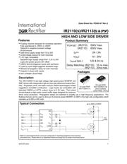
IR2110(S)/IR2113(S) & (PbF)
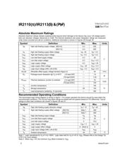
Recommended Operating Conditions
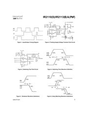
The input/output logic timing diagram is shown in figure 1. For proper operation the device should be used within the
recommended conditions. The V
S
and V
SS
offset ratings are tested with all supplies biased at 15V differential. Typical
ratings at other bias conditions are shown in figures 36 and 37.
Note 1: Logic operational for V
S
of -4 to +500V. Logic state held for V
S
of -4V to -V
BS
. (Please refer to the Design Tip
DT97-3 for more details).
Note 2: When V
DD
< 5V, the minimum V
SS
offset is limited to -V
DD.
Absolute Maximum Ratings
Absolute maximum ratings indicate sustained limits beyond which damage to the device may occur. All voltage param-
eters are absolute voltages referenced to COM. The thermal resistance and power dissipation ratings are measured
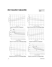
under board mounted and still air conditions. Additional information is shown in Figures 28 through 35.
Symbol Definition Min. Max. Units
V
B
High side floating supply voltage (IR2110) -0.3 525
(IR2113) -0.3 625
V
S
High side floating supply offset voltage V
B
- 25 V
B
+ 0.3
V
HO
High side floating output voltage V
S
- 0.3 V
B
+ 0.3
V
CC
Low side fixed supply voltage -0.3 25
V
LO
Low side output voltage -0.3 V
CC
+ 0.3
V
DD
Logic supply voltage -0.3 V
SS
+ 25
V
SS
Logic supply offset voltage V
CC
- 25 V
CC
+ 0.3
V
IN
Logic input voltage (HIN, LIN & SD) V
SS
- 0.3 V
DD
+ 0.3
dV
s
/dt Allowable offset supply voltage transient (figure 2) — 50 V/ns
P
D
Package power dissipation @ T
A
≤ +25°C (14 lead DIP) — 1.6
(16 lead SOIC) — 1.25
R
THJA
Thermal resistance, junction to ambient (14 lead DIP) — 75
(16 lead SOIC) — 100
T
J
Junction temperature — 150
T
S
Storage temperature -55 150
T
L
Lead temperature (soldering, 10 seconds) — 300
°C/W
W
V
°C
Symbol Definition Min. Max. Units
V
B
High side floating supply absolute voltage V
S
+ 10 V
S
+ 20
V
S
High side floating supply offset voltage (IR2110) Note 1 500
(IR2113) Note 1 600
V
HO
High side floating output voltage V
S
V
B
V
CC
Low side fixed supply voltage 10 20
V
LO
Low side output voltage 0 VCC
V
DD
Logic supply voltage V
SS
+ 3 V
SS
+ 20
V
SS
Logic supply offset voltage -5 (Note 2) 5
V
IN
Logic input voltage (HIN, LIN & SD) V
SS
V
DD
T
A
Ambient temperature -40 125 °C
V
器件 Datasheet 文档搜索
AiEMA 数据库涵盖高达 72,405,303 个元件的数据手册,每天更新 5,000 多个 PDF 文件
