Datasheet 搜索 > FET驱动器 > International Rectifier(国际整流器) > IR2110PBF 数据手册 > IR2110PBF 数据手册 3/16 页
 器件3D模型
¥ 10.46
IR2110PBF 数据手册 - International Rectifier(国际整流器)
制造商:
International Rectifier(国际整流器)
分类:
FET驱动器
封装:
PDIP-14
描述:
INTERNATIONAL RECTIFIER IR2110PBF 芯片, 场效应管, MOSFET驱动器, 高/低压侧, DIP-14 新
Pictures:
3D模型
符号图
焊盘图
引脚图
产品图
页面导航:

导航目录
IR2110PBF数据手册
Page:
of 16 Go
若手册格式错乱,请下载阅览PDF原文件
www.irf.com 3
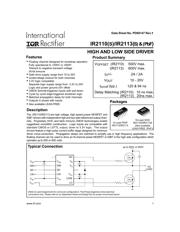
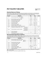
IR2110(S)/IR2113(S) & (PbF)
Symbol Definition Figure Min. Typ. Max. Units Test Conditions
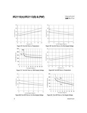
t
on
Turn-on propagation delay 7 — 120 150 V
S
= 0V
t
off
Turn-off propagation delay 8 — 94 125 V
S
= 500V/600V
t
sd
Shutdown propagation delay 9 — 110 140 V
S
= 500V/600V
t
r
Turn-on rise time 10 — 25 35
t
f
Turn-off fall time 11 — 17 25
MT Delay matching, HS & LS (IR2110) — — — 10
turn-on/off (IR2113) — — — 20
ns
Dynamic Electrical Characteristics
V
BIAS
(V
CC
, V
BS
, V
DD
) = 15V, C
L
= 1000 pF, T
A
= 25°C and V
SS
= COM unless otherwise specified. The dynamic
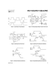
electrical characteristics are measured using the test circuit shown in Figure 3.
Symbol Definition Figure Min. Typ. Max. Units Test Conditions
V
IH
Logic “1” input voltage 12 9.5 — —
V
IL
Logic “0” input voltage 13 — — 6.0
V
OH
High level output voltage, V
BIAS
- V
O
14 — — 1.2 I
O
= 0A
V
OL
Low level output voltage, V
O
15 — — 0.1 I
O
= 0A
I
LK
Offset supply leakage current 16 — — 50 V
B
=V
S
= 500V/600V
I
QBS
Quiescent V
BS
supply current 17 — 125 230 V
IN
= 0V or V
DD
I
QCC
Quiescent V
CC
supply current 18 — 180 340 V
IN
= 0V or V
DD
I
QDD
Quiescent V
DD
supply current 19 — 15 30 V
IN
= 0V or V
DD
I
IN+
Logic “1” input bias current 20 — 20 40 V
IN
= V
DD
I
IN-
Logic “0” input bias current 21 — — 1.0 V
IN
= 0V
V
BSUV+
V
BS
supply undervoltage positive going 22 7.5 8.6 9.7
threshold
V
BSUV-
V
BS
supply undervoltage negative going 23 7.0 8.2 9.4
threshold
V
CCUV+
V
CC
supply undervoltage positive going 24 7.4 8.5 9.6
threshold
V
CCUV-
V
CC
supply undervoltage negative going 25 7.0 8.2 9.4
threshold
I
O+
Output high short circuit pulsed current 26 2.0 2.5 — V
O
= 0V, V
IN
= V
DD
PW ≤ 10 µs
I
O-
Output low short circuit pulsed current 27 2.0 2.5 — V
O
= 15V, V
IN
= 0V
PW ≤ 10 µs
Static Electrical Characteristics
V
BIAS
(V
CC
, V
BS
, V
DD
) = 15V, T
A
= 25°C and V
SS
= COM unless otherwise specified. The V
IN
, V
TH
and I
IN
parameters
are referenced to V
SS
and are applicable to all three logic input leads: HIN, LIN and SD. The V
O
and I
O
parameters are
referenced to COM and are applicable to the respective output leads: HO or LO.
V
µA
V
A
器件 Datasheet 文档搜索
AiEMA 数据库涵盖高达 72,405,303 个元件的数据手册,每天更新 5,000 多个 PDF 文件
