Datasheet 搜索 > MOS管 > Infineon(英飞凌) > IRF9410PBF 数据手册 > IRF9410PBF 数据手册 2/7 页
 器件3D模型
¥ 1.703
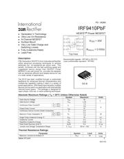
IRF9410PBF 数据手册 - Infineon(英飞凌)
制造商:
Infineon(英飞凌)
分类:
MOS管
封装:
SOIC-8
描述:
INFINEON IRF9410PBF 晶体管, MOSFET, N沟道, 7 A, 30 V, 30 mohm, 10 V, 1 V
Pictures:
3D模型
符号图
焊盘图
引脚图
产品图
页面导航:

导航目录
IRF9410PBF数据手册
Page:
of 7 Go
若手册格式错乱,请下载阅览PDF原文件
IRF9410PbF
2 www.irf.com
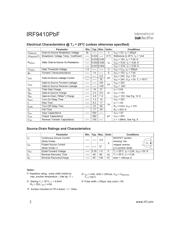
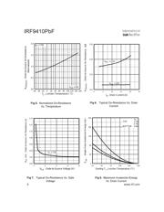
Parameter Min. Typ. Max. Units Conditions
V
(BR)DSS
Drain-to-Source Breakdown Voltage 30 V V
GS
= 0V, I
D
= 250µA
∆V
(BR)DSS
/∆T
J
Breakdown Voltage Temp. Coefficient 0.024 V/°C Reference to 25°C, I
D
= 1mA
0.024 0.030 V
GS
= 10V, I
D
= 7.0A
0.032 0.040 Ω V
GS
= 5.0V, I
D
= 4.0A
0.037 0.050 V
GS
= 4.5V, I
D
= 3.5A
V
GS(th)
Gate Threshold Voltage 1.0 V V
DS
= V
GS
, I
D
= 250µA
g
fs
Forward Transconductance 14 S V
DS
= 15V, I
D
= 7.0A
2.0
µA
V
DS
= 24V, V
GS
= 0V
25 V
DS
= 24V, V
GS
= 0V, T
J
= 55°C
Gate-to-Source Forward Leakage 100
nA
V
GS
= 20V
Gate-to-Source Reverse Leakage -100 V
GS
= -20V
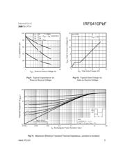
Q
g
Total Gate Charge 18 27 I
D
= 2.0A
Q
gs
Gate-to-Source Charge 2.4 3.6 nC V
DS
= 15V
Q
gd
Gate-to-Drain ("Miller") Charge 4.9 7.4 V
GS
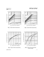
= 10V, See Fig. 10
t
d(on)
Turn-On Delay Time 7.3 15 V
DD
= 25V
t
r
Rise Time 8.3 17
ns
I
D
= 1.0A
t
d(off)
Turn-Off Delay Time 23 46 R
G
= 6.0Ω, V
GS
= 10V
t
f
Fall Time 17 34 R
D
= 25Ω
C
iss
Input Capacitance 550 V
GS
= 0V
C
oss
Output Capacitance 260 pF V
DS
= 25V
C
rss
Reverse Transfer Capacitance 100 = 1.0MHz, See Fig. 9
Parameter Min. Typ. Max. Units Conditions
I
S
Continuous Source Current MOSFET symbol
(Body Diode) showing the
I
SM
Pulsed Source Current integral reverse
(Body Diode) p-n junction diode.
V
SD
Diode Forward Voltage 0.78 1.0 V T
J
= 25°C, I
S
= 2.0A, V
GS
= 0V
t
rr
Reverse Recovery Time 40 80 ns T
J
= 25°C, I
F
= 2.0A
Q
rr
Reverse RecoveryCharge 63 130 nC di/dt = 100A/µs
Source-Drain Ratings and Characteristics
37
2.8
A
S
D
G
Surface mounted on FR-4 board, t ≤ 10sec.
Repetitive rating; pulse width limited by
max. junction temperature. ( See fig. 11 )
I
SD
≤ 4.6A, di/dt ≤ 120A/µs, V
DD
≤ V
(BR)DSS
,
T
J
≤ 150°C
Notes:
Starting T
J
= 25°C, L = 6.6mH
R
G
= 25Ω, I
AS
= 4.6A.
Pulse width ≤ 300µs; duty cycle ≤ 2%.
Electrical Characteristics @ T
J
= 25°C (unless otherwise specified)
I
GSS
I
DSS
Drain-to-Source Leakage Current
R
DS(on)
Static Drain-to-Source On-Resistance
器件 Datasheet 文档搜索
AiEMA 数据库涵盖高达 72,405,303 个元件的数据手册,每天更新 5,000 多个 PDF 文件
