Datasheet 搜索 > DC/DC转换器 > TI(德州仪器) > LMR12007YMK 数据手册 > LMR12007YMK 数据手册 3/30 页

¥ 9.988
LMR12007YMK 数据手册 - TI(德州仪器)
制造商:
TI(德州仪器)
分类:
DC/DC转换器
封装:
TSOT-23-6
描述:
TEXAS INSTRUMENTS LMR12007YMK 直流-直流开关降压(逐步递减)稳压器, 可调, 3V-18V输入, 1.25V-16V输出, 750mA输出, SOT-6
Pictures:
3D模型
符号图
焊盘图
引脚图
产品图
页面导航:
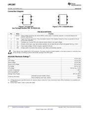
引脚图在P2Hot
典型应用电路图在P1
原理图在P7P8
封装尺寸在P24P26P27
标记信息在P24
封装信息在P24P25P26P27
焊接温度在P2
技术参数、封装参数在P2P3
应用领域在P1
电气规格在P3P4P5P6
导航目录
LMR12007YMK数据手册
Page:
of 30 Go
若手册格式错乱,请下载阅览PDF原文件
LMR12007
www.ti.com
SNVS982 –SEPTEMBER 2013
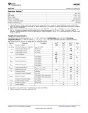
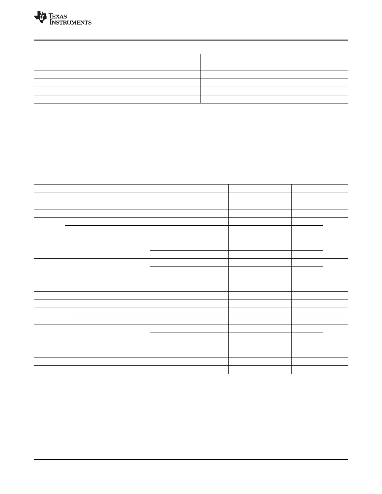
Operating Ratings
(1)
V
IN
3V to 18V
SW Voltage -0.5V to 18V
Boost Voltage -0.5V to 23V
Boost to SW Voltage 1.6V to 5.5V
Junction Temperature Range −40°C to +125°C
Thermal Resistance θ
JA
(2)
118°C/W
(1) Absolute Maximum Ratings indicate limits beyond which damage to the device may occur. Operating Ratings indicate conditions for
which the device is intended to be functional, but specific performance is not ensured. For specific specifications and the test conditions,
see Electrical Characteristics.
(2) Thermal shutdown will occur if the junction temperature exceeds 165°C. The maximum power dissipation is a function of T
J(MAX)
, θ
JA
and T
A
. The maximum allowable power dissipation at any ambient temperature is P
D
= (T
J(MAX)
– T
A
)/θ
JA
. All numbers apply for
packages soldered directly onto a 3” x 3” PC board with 2oz. copper on 4 layers in still air. For a 2 layer board using 1 oz. copper in still
air, θ
JA
= 204°C/W.
Electrical Characteristics
Specifications with standard typeface are for T
J
= 25°C, and those in boldface type apply over the full Operating
Temperature Range (T
J
= -40°C to 125°C). V
IN
= 5V, V
BOOST
- V
SW
= 5V unless otherwise specified. Datasheet min/max
specification limits are ensured by design, test, or statistical analysis.
Symbol Parameter Conditions Min
(1)
Typ
(2)
Max
(1)
Units
V
FB
Feedback Voltage 1.225 1.250 1.275 V
ΔV
FB
/ΔV
IN
Feedback Voltage Line Regulation V
IN
= 3V to 18V 0.01 % / V
I
FB
Feedback Input Bias Current Sink/Source 10 250 nA
Undervoltage Lockout V
IN
Rising 2.74 2.90
UVLO Undervoltage Lockout V
IN
Falling 2.0 2.3 V
UVLO Hysteresis 0.30 0.44 0.62
LMR12007X 1.2 1.6 1.9
F
SW
Switching Frequency MHz
LMR12007Y 0.40 0.55 0.66
LMR12007X 85 92
D
MAX
Maximum Duty Cycle %
LMR12007Y 90 96
LMR12007X 2
D
MIN
Minimum Duty Cycle %
LMR12007Y 1
R
DS(ON)
Switch ON Resistance V
BOOST
- V
SW
= 3V 350 650 mΩ
I
CL
Switch Current Limit V
BOOST
- V
SW
= 3V 1.0 1.5 2.3 A
I
Q
Quiescent Current Switching 1.5 2.5 mA
Quiescent Current (shutdown) V
EN
= 0V 30 nA
LMR12007X (50% Duty Cycle) 2.2 3.3
I
BOOST
Boost Pin Current mA
LMR12007Y (50% Duty Cycle) 0.9 1.6
Shutdown Threshold Voltage V
EN
Falling 0.4
V
EN_TH
V
Enable Threshold Voltage V
EN
Rising 1.8
I
EN
Enable Pin Current Sink/Source 10 nA
I
SW
Switch Leakage 40 nA
(1) Specified to Texas Instruments' Average Outgoing Quality Level (AOQL).
(2) Typicals represent the most likely parametric norm.
Copyright © 2013, Texas Instruments Incorporated Submit Documentation Feedback 3
Product Folder Links: LMR12007
器件 Datasheet 文档搜索
AiEMA 数据库涵盖高达 72,405,303 个元件的数据手册,每天更新 5,000 多个 PDF 文件
