Datasheet 搜索 > 稳压芯片 > TI(德州仪器) > LP5907UVE-1.8/NOPB 数据手册 > LP5907UVE-1.8/NOPB 数据手册 13/36 页

¥ 3.529
LP5907UVE-1.8/NOPB 数据手册 - TI(德州仪器)
制造商:
TI(德州仪器)
分类:
稳压芯片
封装:
XFBGA-4
描述:
TEXAS INSTRUMENTS LP5907UVE-1.8/NOPB 固定电压稳压器, LDO, 2.2V至5.5V, 120mV压差, 1.8V输出, 250mA输出, DSBGA-4
Pictures:
3D模型
符号图
焊盘图
引脚图
产品图
页面导航:
引脚图在P3Hot
典型应用电路图在P13
原理图在P1P11
封装尺寸在P20P23P24P25P27P28P29P30P33
焊盘布局在P21P34
标记信息在P23P24P25P26
封装信息在P19P23P24P25P26P27P28P29P30
技术参数、封装参数在P4
应用领域在P1P4P5P13P36
电气规格在P5P6P15
导航目录
LP5907UVE-1.8/NOPB数据手册
Page:
of 36 Go
若手册格式错乱,请下载阅览PDF原文件
EN
IN OUT
GND
1 PF 1 PF
INPUT
ENABLE
GND
OUTPUT
LP5907
Copyright © 2016, Texas Instruments Incorporated
13
LP5907
www.ti.com
SNVS798J –APRIL 2012–REVISED MARCH 2016
Product Folder Links: LP5907
Submit Documentation FeedbackCopyright © 2012–2016, Texas Instruments Incorporated
8 Applications and Implementation
NOTE
Information in the following applications sections is not part of the TI component
specification, and TI does not warrant its accuracy or completeness. TI’s customers are
responsible for determining suitability of components for their purposes. Customers should
validate and test their design implementation to confirm system functionality.
8.1 Application Information
The LP5907 is designed to meet the requirements of RF and analog circuits, by providing low noise, high PSRR,
low quiescent current, and low line or load transient response figures. The device offers excellent noise
performance without the need for a noise bypass capacitor and is stable with input and output capacitors with a
value of 1 µF. The LP5907 delivers this performance in industry standard packages such as DSBGA, X2SON,
and SOT-23 which, for this device, are specified with an operating junction temperature (T
J
) of –40°C to 125°C.
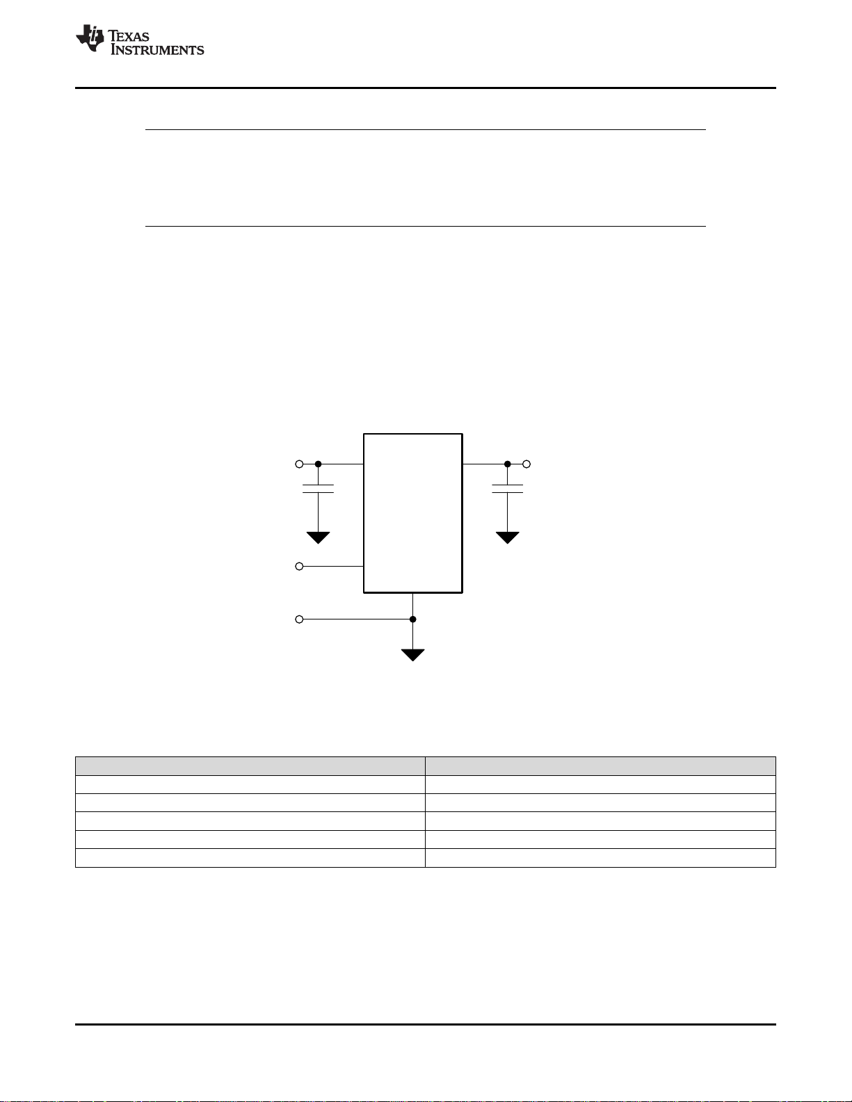
8.2 Typical Application
Figure 21 shows the typical application circuit for the LP5907. Input and output capacitances may need to be
increased above the 1 µF minimum for some applications.
Figure 21. LP5907 Typical Application
8.2.1 Design Requirements
DESIGN PARAMETER EXAMPLE VALUE
Input voltage range 2.2 V to 5.5 V
Output voltage 1.8 V
Output current 200 mA
Output capacitor range 0.7 µF to 10 µF
Input/Output capacitor ESR range 5 to 500 mΩ
8.2.2 Detailed Design Procedure
8.2.2.1 Power Dissipation and Device Operation
The permissible power dissipation for any package is a measure of the capability of the device to pass heat from
the power source, the junctions of the IC, to the ultimate heat sink, the ambient environment. Thus, the power
dissipation is dependent on the ambient temperature and the thermal resistance across the various interfaces
between the die junction and ambient air.
器件 Datasheet 文档搜索
AiEMA 数据库涵盖高达 72,405,303 个元件的数据手册,每天更新 5,000 多个 PDF 文件
