Datasheet 搜索 > 稳压芯片 > TI(德州仪器) > LP5907UVE-1.8/NOPB 数据手册 > LP5907UVE-1.8/NOPB 数据手册 17/36 页

¥ 3.533
LP5907UVE-1.8/NOPB 数据手册 - TI(德州仪器)
制造商:
TI(德州仪器)
分类:
稳压芯片
封装:
XFBGA-4
描述:
TEXAS INSTRUMENTS LP5907UVE-1.8/NOPB 固定电压稳压器, LDO, 2.2V至5.5V, 120mV压差, 1.8V输出, 250mA输出, DSBGA-4
Pictures:
3D模型
符号图
焊盘图
引脚图
产品图
页面导航:
引脚图在P3Hot
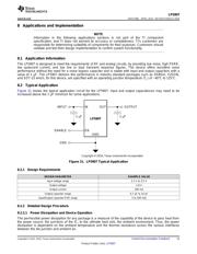
典型应用电路图在P13
原理图在P1P11
封装尺寸在P20P23P24P25P27P28P29P30P33
焊盘布局在P21P34
标记信息在P23P24P25P26
封装信息在P19P23P24P25P26P27P28P29P30
技术参数、封装参数在P4
应用领域在P1P4P5P13P36
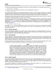
电气规格在P5P6P15
导航目录
LP5907UVE-1.8/NOPB数据手册
Page:
of 36 Go
若手册格式错乱,请下载阅览PDF原文件
V
IN
V
OUT
Power Ground
V
EN
C
IN
C
OUT
LP5907SN
1
2
3
4
IN
GND
EN
OUT
N/C
C
IN
C
OUT
1
2
3
4
5
V
IN
GND
Enable
V
OUT
GND
17
LP5907
www.ti.com
SNVS798J –APRIL 2012–REVISED MARCH 2016
Product Folder Links: LP5907
Submit Documentation FeedbackCopyright © 2012–2016, Texas Instruments Incorporated
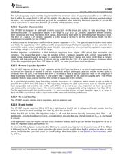
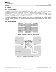
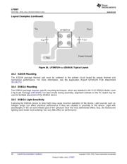
10 Layout
10.1 Layout Guidelines
The dynamic performance of the LP5907 is dependant on the layout of the PCB. PCB layout practices that are
adequate for typical LDOs may degrade the PSRR, noise, or transient performance of the LP5907.
Best performance is achieved by placing C
IN
and C
OUT
on the same side of the PCB as the LP5907, and as
close to the package as is practical. The ground connections for C
IN
and C
OUT
must be back to the LP5907
ground pin using as wide and short a copper trace as is practical.
Connections using long trace lengths, narrow trace widths, and/or connections through vias must be avoided.
These add parasitic inductances and resistance that results in inferior performance especially during transient
conditions
10.2 Layout Examples
Figure 24. LP5907MF-x.x (SOT-23) Typical Layout
Figure 25. LP5907SN-xx (X2SON) Typical Layout
器件 Datasheet 文档搜索
AiEMA 数据库涵盖高达 72,405,303 个元件的数据手册,每天更新 5,000 多个 PDF 文件
