Datasheet 搜索 > NXP(恩智浦) > LPC11U68JBD48K 数据手册 > LPC11U68JBD48K 数据手册 12/97 页

¥ 20.934
LPC11U68JBD48K 数据手册 - NXP(恩智浦)
制造商:
NXP(恩智浦)
封装:
-
描述:
单片机(MCU/MPU/SOC) LPC11U68JBD48K LQFP-48(7x7)
Pictures:
3D模型
符号图
焊盘图
引脚图
产品图
页面导航:
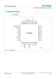
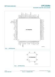
引脚图在P7P9P10P11P12P13P14P15P16P17P18P30Hot
原理图在P6
封装尺寸在P86P87P88
型号编码规则在P4
标记信息在P5
焊接温度在P89P90P91
功能描述在P1P19
技术参数、封装参数在P94
应用领域在P3P56P94
导航目录
LPC11U68JBD48K数据手册
Page:
of 97 Go
若手册格式错乱,请下载阅览PDF原文件
LPC11U6x All information provided in this document is subject to legal disclaimers. © NXP Semiconductors N.V. 2016. All rights reserved.
Product data sheet Rev. 1.3 — 7 September 2016 12 of 97
NXP Semiconductors
LPC11U6x
32-bit ARM Cortex-M0+ microcontroller
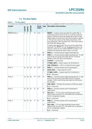
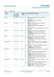
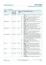
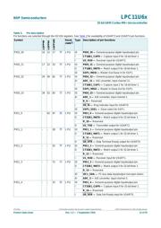
PIO0_20
10 12 17
[6]
I; PU IO PIO0_20 — General-purpose digital input/output pin.
I CT16B1_CAP0 — Capture input 0 for 16-bit timer 1.
I U2_RXD — Receiver input for USART2.
PIO0_21
17 22 33
[6]
I; PU IO PIO0_21 — General-purpose digital input/output pin.
O CT16B1_MAT0 — Match output 0 for 16-bit timer 1.
IO SSP1_MOSI — Master Out Slave In for SSP1.
PIO0_22
29 40 62
[3]
I; PU IO PIO0_22 — General-purpose digital input/output pin.
AI ADC_11 — A/D converter, input channel 11.
I CT16B1_CAP1 — Capture input 1 for 16-bit timer 1.
IO SSP1_MISO — Master In Slave Out for SSP1.
PIO0_23
39 52 83
[3]
I; PU IO PIO0_23 — General-purpose digital input/output pin.
AI ADC_1 — A/D converter, input channel 1.
- R_9 — Reserved.
I U0_RI
— Ring Indicator input for USART0.
IO SSP1_SSEL — Slave select for SSP1.
PIO1_0
-6297
[6]
I; PU IO PIO1_0 — General-purpose digital input/output pin.
O CT32B1_MAT0 — Match output 0 for 32-bit timer 1.
- R_10 — Reserved.
O U2_TXD — Transmitter output for USART2.
PIO1_1
--28
[6]
I; PU IO PIO1_1 — General-purpose digital input/output pin.
O CT32B1_MAT1 — Match output 1 for 32-bit timer 1.
- R_11 — Reserved.
O U0_DTR
— Data Terminal Ready output for USART0.
PIO1_2
--55
[6]
I; PU IO PIO1_2 — General-purpose digital input/output pin.
O CT32B1_MAT2 — Match output 2 for 32-bit timer 1.
- R_12 — Reserved.
I U1_RXD — Receiver input for USART1.
PIO1_3
--72
[3]
I; PU IO PIO1_3 — General-purpose digital input/output pin.
O CT32B1_MAT3 — Match output 3 for 32-bit timer 1.
- R_13 — Reserved.
IO I2C1_SDA — I
2
C-bus data input/output (not open-drain).
AI ADC_5 — A/D converter, input channel 5.
PIO1_4
--23
[6]
I; PU IO PIO1_4 — General-purpose digital input/output pin.
I CT32B1_CAP0 — Capture input 0 for 32-bit timer 1.
- R_14 — Reserved.
I U0_DSR
— Data Set Ready input for USART0.
Table 3. Pin description
Pin functions are selected through the IOCON registers. See Table 2 for availability of USART3 and USART4 pin functions.
Symbol
LQFP48
LQFP64
LQFP100
Reset
state
[1]
Type Description of pin functions
器件 Datasheet 文档搜索
AiEMA 数据库涵盖高达 72,405,303 个元件的数据手册,每天更新 5,000 多个 PDF 文件
