Datasheet 搜索 > NXP(恩智浦) > LPC11U68JBD48K 数据手册 > LPC11U68JBD48K 数据手册 9/97 页

¥ 20.934
LPC11U68JBD48K 数据手册 - NXP(恩智浦)
制造商:
NXP(恩智浦)
封装:
-
描述:
单片机(MCU/MPU/SOC) LPC11U68JBD48K LQFP-48(7x7)
Pictures:
3D模型
符号图
焊盘图
引脚图
产品图
页面导航:
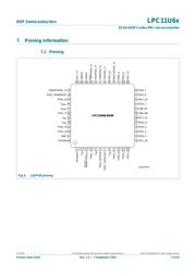
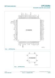
引脚图在P7P9P10P11P12P13P14P15P16P17P18P30Hot
原理图在P6
封装尺寸在P86P87P88
型号编码规则在P4
标记信息在P5
焊接温度在P89P90P91
功能描述在P1P19
技术参数、封装参数在P94
应用领域在P3P56P94
导航目录
LPC11U68JBD48K数据手册
Page:
of 97 Go
若手册格式错乱,请下载阅览PDF原文件
LPC11U6x All information provided in this document is subject to legal disclaimers. © NXP Semiconductors N.V. 2016. All rights reserved.
Product data sheet Rev. 1.3 — 7 September 2016 9 of 97
NXP Semiconductors
LPC11U6x
32-bit ARM Cortex-M0+ microcontroller
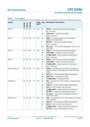
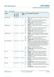
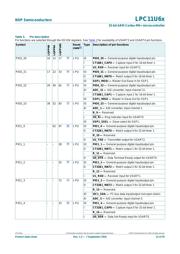
7.2 Pin description
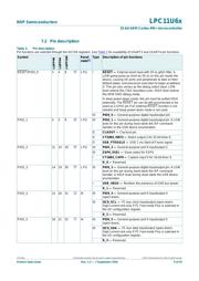
Table 3. Pin description
Pin functions are selected through the IOCON registers. See Table 2 for availability of USART3 and USART4 pin functions.
Symbol
LQFP48
LQFP64
LQFP100
Reset
state
[1]
Type Description of pin functions
RESET/PIO0_0
348
[8]
I; PU I RESET — External reset input with 20 ns glitch filter. A
LOW-going pulse as short as 50 ns on this pin resets the
device, causing I/O ports and peripherals to take on their
default states, and processor execution to begin at address
0. This pin also serves as the debug select input. LOW
level selects the JTAG boundary scan. HIGH level selects
the ARM SWD debug mode.
In deep power-down mode, this pin must be pulled HIGH
externally. The RESET
pin can be left unconnected or be
used as a GPIO pin if an external RESET function is not
needed and Deep power-down mode is not used.
IO PIO0_0 — General-purpose digital input/output pin.
PIO0_1
459
[6]
I; PU IO PIO0_1 — General-purpose digital input/output pin. A LOW
level on this pin during reset starts the ISP command
handler or the USB device enumeration.
O CLKOUT — Clockout pin.
O CT32B0_MAT2 — Match output 2 for 32-bit timer 0.
O USB_FTOGGLE — USB 1 ms Start-of-Frame signal.
PIO0_2
11 14 19
[6]
I; PU IO PIO0_2 — General-purpose port 0 input/output 2.
IO SSP0_SSEL — Slave select for SSP0.
I CT16B0_CAP0 — Capture input 0 for 16-bit timer 0.
- R_0 — Reserved.
PIO0_3
14 19 30
[6]
I; PU IO PIO0_3 — General-purpose digital input/output pin. A LOW
level on this pin during reset starts the ISP command
handler. A HIGH level during reset starts the USB device
enumeration.
I USB_VBUS — Monitors the presence of USB bus power.
- R_1 — Reserved.
PIO0_4
15 20 31
[7]
IA IO PIO0_4 — General-purpose port 0 input/output 4
(open-drain).
IO I2C0_SCL — I
2
C-bus clock input/output (open-drain).
High-current sink only if I
2
C Fast-mode Plus is selected in
the I/O configuration register.
- R_2 — Reserved.
PIO0_5
16 21 32
[7]
IA IO PIO0_5 — General-purpose port 0 input/output 5
(open-drain).
IO I2C0_SDA — I
2
C-bus data input/output (open-drain).
High-current sink only if I
2
C Fast-mode Plus is selected in
the I/O configuration register.
- R_3 — Reserved.
器件 Datasheet 文档搜索
AiEMA 数据库涵盖高达 72,405,303 个元件的数据手册,每天更新 5,000 多个 PDF 文件
