Datasheet 搜索 > ADI(亚德诺) > LT1169CS8#TR 数据手册 > LT1169CS8#TR 数据手册 4/12 页

 器件3D模型
¥ 32.337
LT1169CS8#TR 数据手册 - ADI(亚德诺)
制造商:
ADI(亚德诺)
封装:
SOP
Pictures:
3D模型
符号图
焊盘图
引脚图
产品图
页面导航:
典型应用电路图在P10P11P12
技术参数、封装参数在P1
应用领域在P10P11P12
导航目录
LT1169CS8#TR数据手册
Page:
of 12 Go
若手册格式错乱,请下载阅览PDF原文件
4
LT1169
E
LECTR
IC
AL C CHARA TERIST
ICS
V
S
= ±15V, V
CM
= 0V, –40°C ≤ T
A
≤ 85°C, (Note 7), unless otherwise noted.
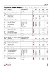
SYMBOL PARAMETER CONDITIONS (Note 1) MIN TYP MAX UNITS
∆V
OS
Offset Voltage Match ● 1.8 6 mV
∆I
B
+
Noninverting Bias Current Match ● 10 180 pA
∆CMRR Common Mode Rejection Match (Note 8) ● 73 93 dB
∆PSRR Power Supply Rejection Match (Note 8) ● 75 92 dB
The ● denotes specifications which apply over the full operating
temperature range.
Note 1: Typical parameters are defined as the 60% yield of parameter
distributions of individual amplifiers, i.e., out of 100 LT1169s (200 op
amps) typically 120 op amps will be better than the indicated specification.
Note 2: I
B
and I
OS
readings are extrapolated to a warmed-up temperature
from 25°C measurements and 45°C characterization data.
Note 3: Current noise is calculated from the formula:
i
n
= (2qI
B
)
1/2
where q = 1.6 × 10
–19
coulomb. The noise of source resistors up to 200M
swamps the contribution of current noise.
Note 4: Input voltage range functionality is assured by testing offset
voltage at the input voltage range limits to a maximum of 2.8mV.
Note 5: This parameter is not 100% tested.
Note 6: Slew rate is measured in A
V
= –1; input signal is ±7.5V, output
measured at ±2.5V.
Note 7: The LT1169 is designed, characterized and expected to meet these
extended temperature limits, but is not tested at –40°C and 85°C.
Guaranteed I grade parts are available; consult factory.
Note 8: ∆CMRR and ∆PSRR are defined as follows:
(1) CMRR and PSRR are measured in µV/V on the individual
amplifiers.
(2) The difference is calculated between the matching sides in µV/V.
(3) The result is converted to dB.
Note 9: The LT1169 is measured in an automated tester in less than one
second after application of power. Depending on the package used, power
dissipation, heat sinking, and air flow conditions, the fully warmed-up chip
temperature can be 10°C to 50°C higher than the ambient temperature.
CCHARA TERIST
ICS
UW
AT
Y
P
I
CA
LPER
F
O
R
C
E
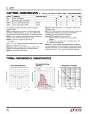
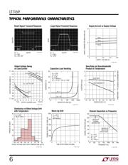
Voltage Noise vs Frequency0.1Hz to 10Hz Voltage Noise
TIME (SEC)
VOLTAGE NOISE (1µV/DIV)
2468
LT1169 • TPC01
100
FREQUENCY (Hz)
1 10
1
10
100
100 1k 10k
LT1169 • TPC03
RMS VOLTAGE NOISE (nV/√Hz)
T
A
= 25°C
V
S
= ±15V
1/f CORNER
60Hz
TYPICAL
INPUT VOLTAGE NOISE (nV/√Hz)
4.2
PERCENT OF UNITS (%)
30
40
50
7.4
LT1169 • TPC02
20
10
0
5.0
5.8
6.6
4.6 7.8
5.4
6.2
7.0
8.2
T
A
= 25°C
V
S
= ±15V
510 OP AMPS TESTED
1kHz Input Noise Voltage
Distribution
器件 Datasheet 文档搜索
AiEMA 数据库涵盖高达 72,405,303 个元件的数据手册,每天更新 5,000 多个 PDF 文件
