Datasheet 搜索 > 稳压芯片 > Microchip(微芯) > MCP1825S-1202E/DB 数据手册 > MCP1825S-1202E/DB 数据手册 19/38 页

¥ 4.69
MCP1825S-1202E/DB 数据手册 - Microchip(微芯)
制造商:
Microchip(微芯)
分类:
稳压芯片
封装:
TO-261-4
描述:
MICROCHIP MCP1825S-1202E/DB 固定电压稳压器, LDO, 2.1V至6V, 210mV压差, 1.2V输出, 500mA输出, SOT-223-3
Pictures:
3D模型
符号图
焊盘图
引脚图
产品图
页面导航:
引脚图在P16Hot
典型应用电路图在P3P19P20P21
原理图在P4P5P6
标记信息在P23P24
封装信息在P23P25P26P28P29P32P35
技术参数、封装参数在P8P9P10
应用领域在P1P3
电气规格在P8P9P18P19
导航目录
MCP1825S-1202E/DB数据手册
Page:
of 38 Go
若手册格式错乱,请下载阅览PDF原文件
© 2008 Microchip Technology Inc. DS22056B-page 19
MCP1825/MCP1825S
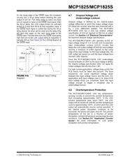
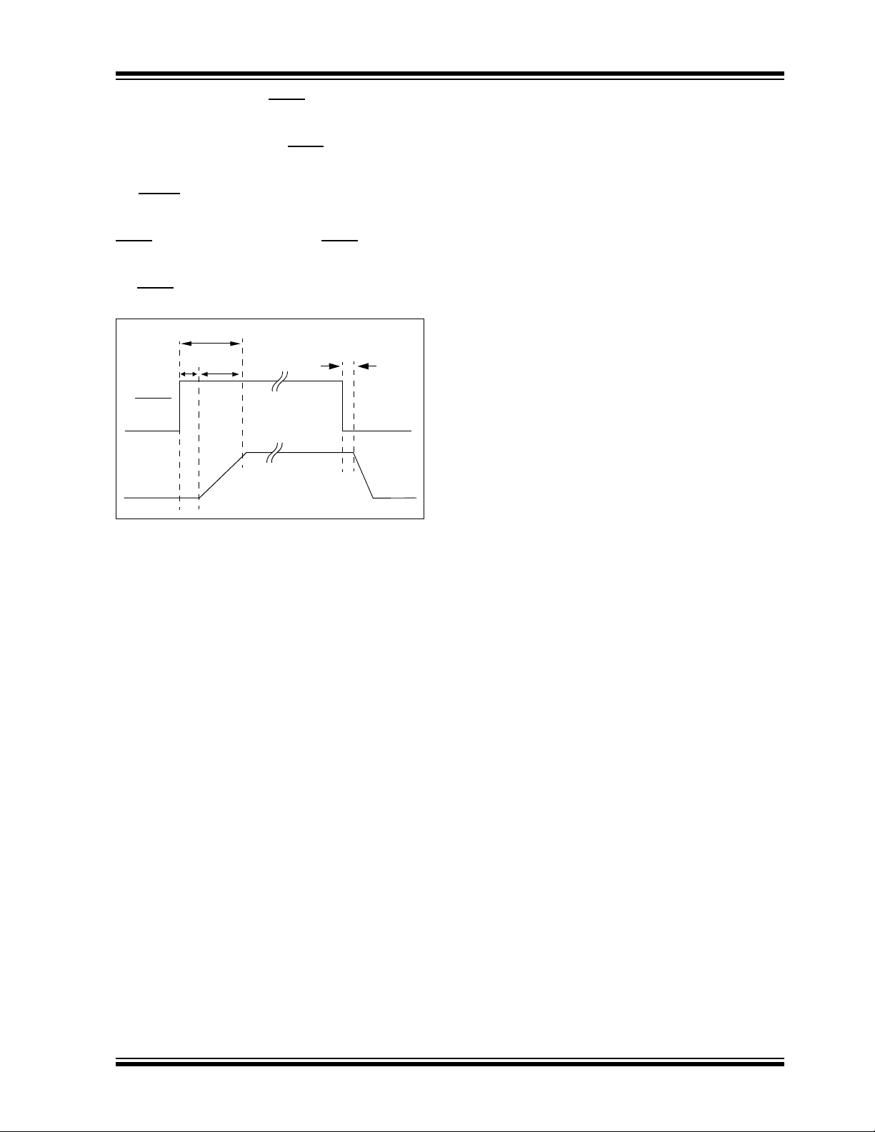
On the rising edge of the SHDN input, the shutdown
circuitry has a 30 µs delay before allowing the LDO
output to turn on. This delay helps to reject any false
turn-on signals or noise on the SHDN
input signal. After
the 30 µs delay, the LDO output enters its soft-start
period as it rises from 0V to its final regulation value. If
the SHDN
input signal is pulled low during the 30 µs
delay period, the timer will be reset and the delay time
will start over again on the next rising edge of the
SHDN
input. The total time from the SHDN input going
high (turn-on) to the LDO output being in regulation is
typically 100 µs. See Figure 4-4 for a timing diagram of
the SHDN
input.
FIGURE 4-4: Shutdown Input Timing
Diagram.
4.7 Dropout Voltage and
Undervoltage Lockout
Dropout voltage is defined as the input-to-output
voltage differential at which the output voltage drops
2% below the nominal value that was measured with a
V
R
+ 0.5V differential applied. The MCP1825/
MCP1825S LDO has a very low dropout voltage
specification of 210 mV (typical) at 500 mA of output
current. See Section 1.0 “Electrical Characteristics”
for maximum dropout voltage specifications.
The MCP1825/MCP1825S LDO operates across an
input voltage range of 2.1V to 6.0V and incorporates
input Undervoltage Lockout (UVLO) circuitry that
keeps the LDO output voltage off until the input voltage
reaches a minimum of 2.00V (typical) on the rising
edge of the input voltage. As the input voltage falls, the
LDO output will remain on until the input voltage level
reaches 1.82V (typical).
Since the MCP1825/MCP1825S LDO undervoltage
lockout activates at 1.82V as the input voltage is falling,
the dropout voltage specification does not apply for
output voltages that are less than 1.8V.
For high-current applications, voltage drops across the
PCB traces must be taken into account. The trace
resistances can cause significant voltage drops
between the input voltage source and the LDO. For
applications with input voltages near 2.1V, these PCB
trace voltage drops can sometimes lower the input
voltage enough to trigger a shutdown due to
undervoltage lockout.
4.8 Overtemperature Protection
The MCP1825/MCP1825S LDO has temperature-
sensing circuitry to prevent the junction temperature
from exceeding approximately 150°C. If the LDO
junction temperature does reach 150°C, the LDO
output will be turned off until the junction temperature
cools to approximately 140°C, at which point the LDO
output will automatically resume normal operation. If
the internal power dissipation continues to be
excessive, the device will again shut off. The junction
temperature of the die is a function of power
dissipation, ambient temperature and package thermal
resistance. See Section 5.0 “Application Circuits/
Issues” for more information on LDO power
dissipation and junction temperature.
SHDN
V
OUT
30 µs
70 µs
T
OR
400 ns (typ)
器件 Datasheet 文档搜索
AiEMA 数据库涵盖高达 72,405,303 个元件的数据手册,每天更新 5,000 多个 PDF 文件
