Datasheet 搜索 > 稳压芯片 > Microchip(微芯) > MCP1825S-1202E/DB 数据手册 > MCP1825S-1202E/DB 数据手册 20/38 页


¥ 4.692
MCP1825S-1202E/DB 数据手册 - Microchip(微芯)
制造商:
Microchip(微芯)
分类:
稳压芯片
封装:
TO-261-4
描述:
MICROCHIP MCP1825S-1202E/DB 固定电压稳压器, LDO, 2.1V至6V, 210mV压差, 1.2V输出, 500mA输出, SOT-223-3
Pictures:
3D模型
符号图
焊盘图
引脚图
产品图
页面导航:
引脚图在P16Hot
典型应用电路图在P3P19P20P21
原理图在P4P5P6
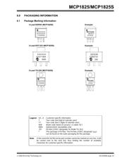
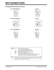
标记信息在P23P24
封装信息在P23P25P26P28P29P32P35
技术参数、封装参数在P8P9P10
应用领域在P1P3
电气规格在P8P9P18P19
导航目录
MCP1825S-1202E/DB数据手册
Page:
of 38 Go
若手册格式错乱,请下载阅览PDF原文件

MCP1825/MCP1825S
DS22056B-page 20 © 2008 Microchip Technology Inc.
5.0 APPLICATION CIRCUITS/
ISSUES
5.1 Typical Application
The MCP1825/MCP1825S is used for applications that
require high LDO output current and a power good
output.
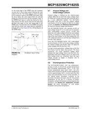
FIGURE 5-1: Typical Application Circuit.
5.1.1 APPLICATION CONDITIONS
5.2 Power Calculations
5.2.1 POWER DISSIPATION
The internal power dissipation within the MCP1825/
MCP1825S is a function of input voltage, output
voltage, output current and quiescent current.
Equation 5-1 can be used to calculate the internal
power dissipation for the LDO.
EQUATION 5-1:
In addition to the LDO pass element power dissipation,
there is power dissipation within the MCP1825/
MCP1825S as a result of quiescent or ground current.
The power dissipation as a result of the ground current
can be calculated using the following equation:
EQUATION 5-2:
The total power dissipated within the MCP1825/
MCP1825S is the sum of the power dissipated in the
LDO pass device and the P(I
GND
) term. Because of the
CMOS construction, the typical I
GND
for the MCP1825/
MCP1825S is 120 µA. Operating at a maximum V
IN
of
3.465V results in a power dissipation of 0.12 milli-Watts
for a 2.5V output. For most applications, this is small
compared to the LDO pass device power dissipation
and can be neglected.
The maximum continuous operating junction
temperature specified for the MCP1825/MCP1825S is
+125°C
. To estimate the internal junction temperature
of the MCP1825/MCP1825S, the total internal power
dissipation is multiplied by the thermal resistance from
junction to ambient (Rθ
JA
) of the device. The thermal
resistance from junction to ambient for the TO-220-5
package is estimated at 29.3°C/W.
EQUATION 5-3:
Package Type = TO-220-5
Input Voltage Range = 3.3V ± 5%
V
IN
maximum = 3.465V
V
IN
minimum = 3.135V
V
DROPOUT (max)
= 0.350V
V
OUT
(typical) = 2.5V
I
OUT
= 500 mA maximum
P
DISS
(typical) = 0.483W
Temperature Rise = 14.2°C
10 µF
V
OUT
= 2.5V @ 500 mA
R
1
C
2
10 kΩ
PWRGD
SHDN
GND
2
4.7 µF
On
Off
C
1
MCP1825-2.5
1
3
4
5
3.3V
V
IN
P
LDO
V
IN MAX )()
V
OUT MIN()
–()I
OUT MAX )()
×=
Where:
P
LDO
= LDO Pass device internal
power dissipation
V
IN(MAX)
= Maximum input voltage
V
OUT(MIN)
= LDO minimum output voltage
P
IGND()
V
IN MAX()
I
VIN
×=
Where:
P
I(GND
= Power dissipation due to the
quiescent current of the LDO
V
IN(MAX)
= Maximum input voltage
I
VIN
= Current flowing in the V
IN
pin
with no LDO output current
(LDO quiescent current)
T
JMAX()
P
TOTAL
Rθ
JA
× T
AMAX
+=
T
J(MAX)
= Maximum continuous junction
temperature
P
TOTAL
= Total device power dissipation
Rθ
JA
= Thermal resistance from junction to
ambient
T
AMAX
= Maximum ambient temperature
器件 Datasheet 文档搜索
AiEMA 数据库涵盖高达 72,405,303 个元件的数据手册,每天更新 5,000 多个 PDF 文件
