Datasheet 搜索 > 双极性晶体管 > ON Semiconductor(安森美) > MMBTA06LT1G 数据手册 > MMBTA06LT1G 数据手册 2/7 页

¥ 0.109
MMBTA06LT1G 数据手册 - ON Semiconductor(安森美)
制造商:
ON Semiconductor(安森美)
分类:
双极性晶体管
封装:
SOT-23-3
描述:
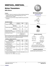
NPN 晶体管,ON Semiconductor这些 ON Semiconductor 双极晶体管可放大模拟或数字信号。 它们还可切换直流或用作振荡器。 ### 标准Manufacturer Part Nos with S or NSV prefix are automotive qualified to AEC-Q101 standard.### 双极性晶体管,On SemiconductorON Semiconductor 的各种双极晶体管,包括以下类别:小信号晶体管 通用晶体管 双 NPN 和 PNP 晶体管 功率晶体管 高电压晶体管 射频双极晶体管 低噪声,双匹配和复杂的双极晶体管
Pictures:
3D模型
符号图
焊盘图
引脚图
产品图
页面导航:
导航目录
MMBTA06LT1G数据手册
Page:
of 7 Go
若手册格式错乱,请下载阅览PDF原文件
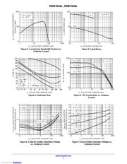
MMBTA05L, MMBTA06L
www.onsemi.com
2
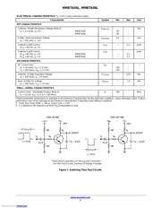
ELECTRICAL CHARACTERISTICS (T
A
= 25°C unless otherwise noted)
Characteristic
Symbol Min Max Unit
OFF CHARACTERISTICS
Collector−Emitter Breakdown Voltage (Note 3)
(I
C
= 1.0 mAdc, I
B
= 0) MMBTA05L
MMBTA06L
V
(BR)CEO
60
80
−
−
Vdc
Emitter−Base Breakdown Voltage
(I
E
= 100 mAdc, I
C
= 0)
V
(BR)EBO
4.0 − Vdc
Collector Cutoff Current
(V
CE
= 60 Vdc, I
B
= 0)
I
CES
− 0.1
mAdc
Collector Cutoff Current
(V
CB
= 60 Vdc, I
E
= 0) MMBTA05L
(V
CB
= 80 Vdc, I
E
= 0) MMBTA06L
I
CBO
−
−
0.1
0.1
mAdc
ON CHARACTERISTICS
DC Current Gain
(I
C
= 10 mAdc, V
CE
= 1.0 Vdc)
(I
C
= 100 mAdc, V
CE
= 1.0 Vdc)
h
FE
100
100
−
−
−
Collector−Emitter Saturation Voltage
(I
C
= 100 mAdc, I
B
= 10 mAdc)
V
CE(sat)
− 0.25 Vdc
Base−Emitter On Voltage
(I
C
= 100 mAdc, V
CE
= 1.0 Vdc)
V
BE(on)
− 1.2 Vdc
SMALL−SIGNAL CHARACTERISTICS
Current−Gain − Bandwidth Product (Note 4)
(I
C
= 10 mA, V
CE
= 2.0 V, f = 100 MHz)
f
T
100 − MHz
Product parametric performance is indicated in the Electrical Characteristics for the listed test conditions, unless otherwise noted. Product
performance may not be indicated by the Electrical Characteristics if operated under different conditions.
3. Pulse Test: Pulse Width v 300 ms, Duty Cycle v 2.0%.
4. f
T
is defined as the frequency at which |h
fe
| extrapolates to unity.
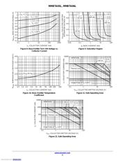
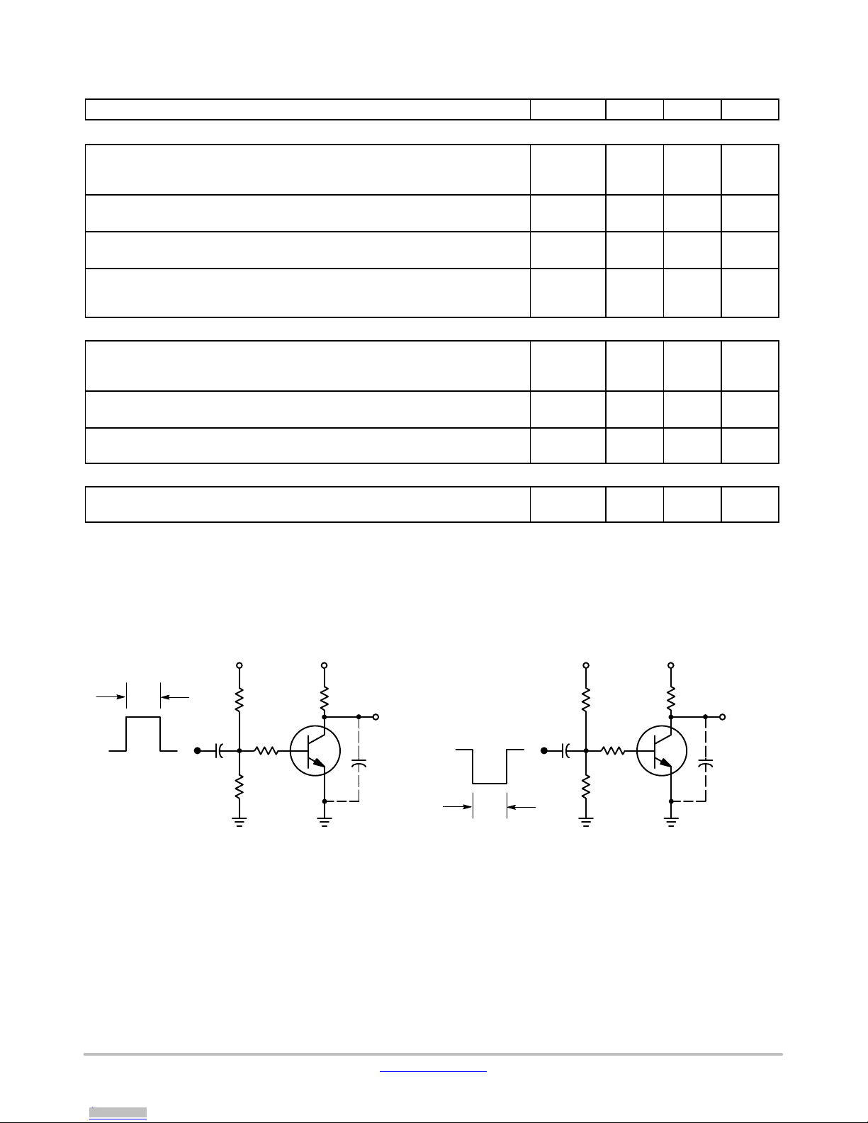
Figure 1. Switching Time Test Circuits
OUTPUT
TURN-ON TIME
-1.0 V
V
CC
+40 V
R
L
* C
S
t 6.0 pF
R
B
100
100
V
in
5.0 mF
t
r
= 3.0 ns
0
+10 V
5.0 ms
OUTPUT
TURN-OFF TIME
+V
BB
V
CC
+40 V
R
L
* C
S
t 6.0 pF
R
B
100
100
V
in
5.0 mF
t
r
= 3.0 ns
5.0 ms
*Total Shunt Capacitance of Test Jig and Connectors
For PNP Test Circuits, Reverse All Voltage Polarities
Downloaded from Arrow.com.Downloaded from Arrow.com.
器件 Datasheet 文档搜索
AiEMA 数据库涵盖高达 72,405,303 个元件的数据手册,每天更新 5,000 多个 PDF 文件
