Datasheet 搜索 > Micron(镁光) > MT41J128M16JT-093:MTR 数据手册 > MT41J128M16JT-093:MTR 数据手册 6/211 页


¥ 0
MT41J128M16JT-093:MTR 数据手册 - Micron(镁光)
制造商:
Micron(镁光)
Pictures:
3D模型
符号图
焊盘图
引脚图
产品图
页面导航:
原理图在P14P15P146
封装尺寸在P22P23P24P25
标记信息在P1P2
功能描述在P12P13P146P192
技术参数、封装参数在P26P27P30P31P32P33P34P35P36P37P38P39
电气规格在P26P27P30P31P32P33P34P35P36P37P38P39
型号编号列表在P2
导航目录
MT41J128M16JT-093:MTR数据手册
Page:
of 211 Go
若手册格式错乱,请下载阅览PDF原文件

List of Figures
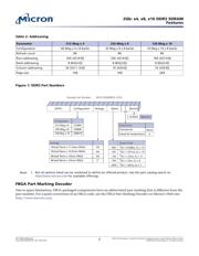
Figure 1: DDR3 Part Numbers .......................................................................................................................... 2
Figure 2: Simplified State Diagram ................................................................................................................. 11
Figure 3: 512 Meg x 4 Functional Block Diagram ............................................................................................. 14
Figure 4: 256 Meg x 8 Functional Block Diagram ............................................................................................. 15
Figure 5: 128 Meg x 16 Functional Block Diagram ........................................................................................... 15
Figure 6: 78-Ball FBGA – x4, x8 (Top View) ...................................................................................................... 16
Figure 7: 96-Ball FBGA – x16 (Top View) ......................................................................................................... 17
Figure 8: 78-Ball FBGA – x4, x8 (DA) ............................................................................................................... 22
Figure 9: 78-Ball FBGA – x4, x8 (HX) ............................................................................................................... 23
Figure 10: 96-Ball FBGA – x16 (HA) ................................................................................................................. 24
Figure 11: 96-Ball FBGA – x16 (JT) .................................................................................................................. 25
Figure 12: Thermal Measurement Point ......................................................................................................... 29
Figure 13: Input Signal .................................................................................................................................. 46
Figure 14: Overshoot ..................................................................................................................................... 47
Figure 15: Undershoot ................................................................................................................................... 47
Figure 16: V
IX
for Differential Signals .............................................................................................................. 49
Figure 17: Single-Ended Requirements for Differential Signals ........................................................................ 49
Figure 18: Definition of Differential AC-Swing and
t
DVAC ............................................................................... 50
Figure 19: Nominal Slew Rate Definition for Single-Ended Input Signals .......................................................... 52
Figure 20: Nominal Differential Input Slew Rate Definition for DQS, DQS# and CK, CK# .................................. 53
Figure 21: ODT Levels and I-V Characteristics ................................................................................................ 54
Figure 22: ODT Timing Reference Load .......................................................................................................... 57
Figure 23:
t
AON and
t
AOF Definitions ............................................................................................................ 58
Figure 24:
t
AONPD and
t
AOFPD Definitions ................................................................................................... 58
Figure 25:
t
ADC Definition ............................................................................................................................. 59
Figure 26: Output Driver ................................................................................................................................ 60
Figure 27: DQ Output Signal .......................................................................................................................... 67
Figure 28: Differential Output Signal .............................................................................................................. 68
Figure 29: Reference Output Load for AC Timing and Output Slew Rate ........................................................... 68
Figure 30: Nominal Slew Rate Definition for Single-Ended Output Signals ....................................................... 69
Figure 31: Nominal Differential Output Slew Rate Definition for DQS, DQS# .................................................... 70
Figure 32: Nominal Slew Rate and
t
VAC for
t
IS (Command and Address – Clock) ............................................. 100
Figure 33: Nominal Slew Rate for
t
IH (Command and Address – Clock) ........................................................... 101
Figure 34: Tangent Line for
t
IS (Command and Address – Clock) .................................................................... 102
Figure 35: Tangent Line for
t
IH (Command and Address – Clock) .................................................................... 103
Figure 36: Nominal Slew Rate and
t
VAC for
t
DS (DQ – Strobe) ......................................................................... 109
Figure 37: Nominal Slew Rate for
t
DH (DQ – Strobe) ...................................................................................... 110
Figure 38: Tangent Line for
t
DS (DQ – Strobe) ................................................................................................ 111
Figure 39: Tangent Line for
t
DH (DQ – Strobe) ............................................................................................... 112
Figure 40: Refresh Mode ............................................................................................................................... 119
Figure 41: DLL Enable Mode to DLL Disable Mode ........................................................................................ 121
Figure 42: DLL Disable Mode to DLL Enable Mode ........................................................................................ 122
Figure 43: DLL Disable
t
DQSCK .................................................................................................................... 123
Figure 44: Change Frequency During Precharge Power-Down ........................................................................ 125
Figure 45: Write Leveling Concept ................................................................................................................. 126
Figure 46: Write Leveling Sequence ............................................................................................................... 129
Figure 47: Write Leveling Exit Procedure ....................................................................................................... 130
Figure 48: Initialization Sequence ................................................................................................................. 132
Figure 49: MRS to MRS Command Timing (
t
MRD) ......................................................................................... 133
Figure 50: MRS to nonMRS Command Timing (
t
MOD) .................................................................................. 134
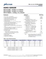
2Gb: x4, x8, x16 DDR3 SDRAM
Features
PDF: 09005aef826aaadc
2Gb_DDR3_SDRAM.pdf - Rev. Q 04/13 EN
6
Micron Technology, Inc. reserves the right to change products or specifications without notice.
2006 Micron Technology, Inc. All rights reserved.
器件 Datasheet 文档搜索
AiEMA 数据库涵盖高达 72,405,303 个元件的数据手册,每天更新 5,000 多个 PDF 文件
