Datasheet 搜索 > 放大器、缓冲器 > ON Semiconductor(安森美) > NE5517NG 数据手册 > NE5517NG 数据手册 4/15 页
 器件3D模型
¥ 0.89
NE5517NG 数据手册 - ON Semiconductor(安森美)
制造商:
ON Semiconductor(安森美)
分类:
放大器、缓冲器
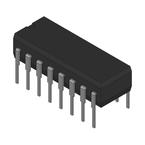
封装:
DIP-16
描述:
双通道互导放大器
Pictures:
3D模型
符号图
焊盘图
引脚图
产品图
页面导航:
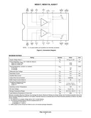
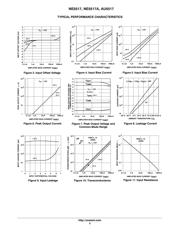
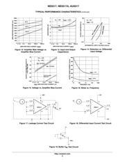
引脚图在P1P2Hot
典型应用电路图在P7
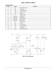
原理图在P2
封装尺寸在P14P15
焊盘布局在P14
型号编码规则在P1P13P15
标记信息在P1P15
封装信息在P13
技术参数、封装参数在P13
应用领域在P1P7P8
电气规格在P4P5P6
导航目录
NE5517NG数据手册
Page:
of 15 Go
若手册格式错乱,请下载阅览PDF原文件
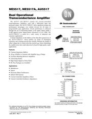
NE5517, NE5517A, AU5517
http://onsemi.com
4
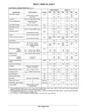
ELECTRICAL CHARACTERISTICS (Note 4)
Characteristic
Test Conditions Symbol
AU5517/NE5517 NE5517A
Unit
Min Typ Max Min Typ Max
Input Offset Voltage
Overtemperature Range
I
ABC
5.0 mA
V
OS
0.4
0.3
5.0
5.0
0.4
0.3
2.0
5.0
2.0
mV
DV
OS
/DT
Avg. TC of Input Offset Voltage 7.0 7.0
mV/°C
V
OS
Including Diodes Diode Bias Current
(I
D
) = 500 mA
0.5 5 0.5 2.0 mV
Input Offset Change
5.0 mA ≤ I
ABC
≤ 500 mA
V
OS
0.1 0.1 3.0 mV
Input Offset Current I
OS
0.1 0.6 0.1 0.6
mA
DI
OS
/DT
Avg. TC of Input Offset Current 0.001 0.001
mA/°C
Input Bias Current
Overtemperature Range
I
BIAS
0.4
1.0
5.0
8.0
0.4
1.0
5.0
7.0
mA
DI
B
/DT
Avg. TC of Input Current 0.01 0.01
mA/°C
Forward Transconductance
Overtemperature Range
g
M
6700
5400
9600 13000 7700
4000
9600 12000
mmho
g
M
Tracking 0.3 0.3 dB
Peak Output Current
R
L
= 0, I
ABC
= 5.0 mA
R
L
= 0, I
ABC
= 500 mA
R
L
= 0, Overtemperature
Range
I
OUT
350
300
5.0
500 650
3.0
350
300
5.0
500
7.0
650
mA
Peak Output Voltage
Positive
Negative
R
L
= ∞, 5.0 mA ≤ I
ABC
≤ 500 mA
R
L
= ∞, 5.0 mA ≤ I
ABC
≤ 500 mA
V
OUT
+12
−12
+14.2
−14.4
+12
−12
+14.2
−14.4
V
Supply Current
I
ABC
= 500 mA, both channels
I
CC
2.6 4.0 2.6 4.0 mA
V
OS
Sensitivity
Positive
Negative
D V
OS
/D V+
D V
OS
/D V−
20
20
150
150
20
20
150
150
mV/V
Common-mode Rejection
Ration
CMRR 80 110 80 110 dB
Common-mode Range ±12 ±13.5 ±12 ±13.5 V
Crosstalk Referred to Input (Note 5)
20 Hz < f < 20 kHz
100 100 dB
Differential Input Current I
ABC
= 0, Input = ±4.0 V I
IN
0.02 100 0.02 10 nA
Leakage Current I
ABC
= 0 (Refer to Test Circuit) 0.2 100 0.2 5.0 nA
Input Resistance R
IN
10 26 10 26
kW
Open-loop Bandwidth B
W
2.0 2.0 MHz
Slew Rate Unity Gain Compensated SR 50 50
V/ms
Buffer Input Current 5 IN
BUFFER
0.4 5.0 0.4 5.0
mA
Peak Buffer Output Voltage 5 VO
BUFFER
10 10 V
DV
BE
of Buffer
Refer to Buffer V
BE
Test
Circuit (Note 6)
0.5 5.0 0.5 5.0 mV
4. These specifications apply for V
S
= ±15 V, T
amb
= 25°C, amplifier bias current (I
ABC
) = 500 mA, Pins 2 and 15 open unless otherwise
specified. The inputs to the buffers are grounded and outputs are open.
5. These specifications apply for V
S
= ±15 V, I
ABC
= 500 mA, R
OUT
= 5.0 kW connected from the buffer output to −V
S
and the input of the buffer
is connected to the transconductance amplifier output.
6. V
S
= ±15, R
OUT
= 5.0 kW connected from Buffer output to −V
S
and 5.0 mA ≤ I
ABC
≤ 500 mA.
器件 Datasheet 文档搜索
AiEMA 数据库涵盖高达 72,405,303 个元件的数据手册,每天更新 5,000 多个 PDF 文件
