Datasheet 搜索 > MOS管 > ON Semiconductor(安森美) > NTGS3455T1 数据手册 > NTGS3455T1 数据手册 1/6 页

¥ 0.875
NTGS3455T1 数据手册 - ON Semiconductor(安森美)
制造商:
ON Semiconductor(安森美)
分类:
MOS管
封装:
SOT-23-6
描述:
-4.5A,-12V功率MOSFET
Pictures:
3D模型
符号图
焊盘图
引脚图
产品图
页面导航:
导航目录
NTGS3455T1数据手册
Page:
of 6 Go
若手册格式错乱,请下载阅览PDF原文件
© Semiconductor Components Industries, LLC, 2006
February, 2006 − Rev. 2
1 Publication Order Number:
NTGS3433T1/D
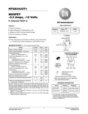
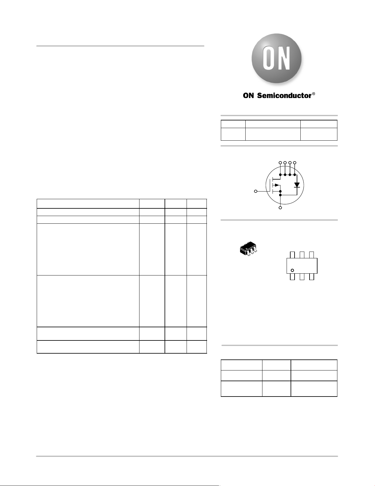
NTGS3433T1
MOSFET
−3.3 Amps, −12 Volts
P−Channel TSOP−6
Features
• Ultra Low R
DS(on)
• Higher Efficiency Extending Battery Life
• Miniature TSOP−6 Surface Mount Package
• Pb−Free Package is Available
Applications
• Power Management in Portable and Battery−Powered Products,
i.e.: Cellular and Cordless Telephones, and PCMCIA Cards
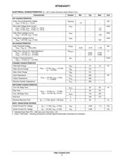
MAXIMUM RATINGS (T
J
= 25°C unless otherwise noted.)
Rating
Symbol Value Unit
Drain−to−Source Voltage V
DSS
−12 Volts
Gate−to−Source Voltage − Continuous V
GS
"8.0 Volts
Thermal Resistance
Junction−to−Ambient (Note 1)
Total Power Dissipation @ T
A
= 25°C
Drain Current
− Continuous @ T
A
= 25°C
− Pulsed Drain Current (T
p
t 10 mS)
Maximum Operating Power Dissipation
Maximum Operating Drain Current
R
q
JA
P
d
I
D
I
DM
P
d
I
D
62.5
2.0
−3.3
−20
1.0
−2.35
°C/W
Watts
Amps
Amps
Watts
Amps
Thermal Resistance
Junction−to−Ambient (Note 2)
Total Power Dissipation @ T
A
= 25°C
Drain Current
− Continuous @ T
A
= 25°C
− Pulsed Drain Current (T
p
t 10 mS)
Maximum Operating Power Dissipation
Maximum Operating Drain Current
R
q
JA
P
d
I
D
I
DM
P
d
I
D
128
1.0
−2.35
−14
0.5
−1.65
°C/W
Watts
Amps
Amps
Watts
Amps
Operating and Storage Temperature Range T
J
, T
stg
−55 to
150
°C
Maximum Lead Temperature for Soldering
Purposes for 10 Seconds
T
L
260 °C
Maximum ratings are those values beyond which device damage can occur.
Maximum ratings applied to the device are individual stress limit values (not
normal operating conditions) and are not valid simultaneously. If these limits are
exceeded, device functional operation is not implied, damage may occur and
reliability may be affected.
1. Mounted onto a 2″ square FR−4 board (1 in sq, 2 oz. Cu 0.06″ thick single
sided), t t 5.0 seconds.
2. Mounted onto a 2″ square FR−4 board (1 in sq, 2 oz. Cu 0.06″ thick single
sided), operating to steady state.
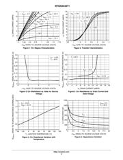
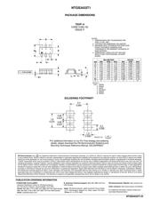
3
4
1256
P−Channel
TSOP−6
CASE 318G
STYLE 1
MARKING DIAGRAM &
PIN ASSIGNMENT
GATE
DRAIN
SOURCE
†For information on tape and reel specifications,
including part orientation and tape sizes, please
refer to our Tape and Reel Packaging Specification
Brochure, BRD8011/D.
Device Package Shipping
†
ORDERING INFORMATION
NTGS3433T1
TSOP−6 3000 Tape & Reel
TSOP−6
(Pb−Free)
3000 Tape & Reel
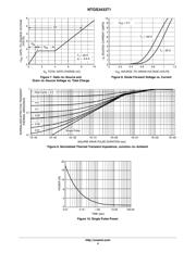
V
(BR)DSS
R
DS(on)
TYP I
D
Max
−12 V
75 mW @ −4.5 V
−3.3 A
1
433 M G
G
433 = Specific Device Code
M
= Date Code*
G = Pb−Free Package
Source
4
Drain
6
Drain
5
3
Gate
1
Drain
2
Drain
(Note: Microdot may be in either location)
*Date Code orientation may vary depending
upon manufacturing location.
NTGS3433T1G
http://onsemi.com
器件 Datasheet 文档搜索
AiEMA 数据库涵盖高达 72,405,303 个元件的数据手册,每天更新 5,000 多个 PDF 文件
