Datasheet 搜索 > 微控制器 > Microchip(微芯) > PIC18F4685-E/ML 数据手册 > PIC18F4685-E/ML 数据手册 165/484 页

 器件3D模型
¥ 34.818
PIC18F4685-E/ML 数据手册 - Microchip(微芯)
制造商:
Microchip(微芯)
分类:
微控制器
封装:
QFN-44
描述:
PIC18 系列 3328 B RAM 96 kB 闪存 8位 微控制器 - QFN-44
Pictures:
3D模型
符号图
焊盘图
引脚图
产品图
页面导航:
引脚图在P4P5P167P169P176Hot
典型应用电路图在P193
原理图在P10P12P13P27P43P146P150P154P160P162P168P169
封装尺寸在P459
标记信息在P457P458
封装信息在P457P459P460P461P462P463
技术参数、封装参数在P432P433P434P436P437P438
应用领域在P180P272
电气规格在P107P260P261P265P266
导航目录
PIC18F4685-E/ML数据手册
Page:
of 484 Go
若手册格式错乱,请下载阅览PDF原文件

© 2007 Microchip Technology Inc. Preliminary DS39761B-page 163
PIC18F2682/2685/4682/4685
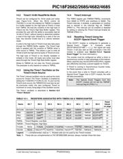
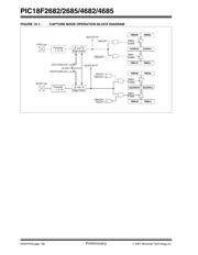
15.0 CAPTURE/COMPARE/PWM
(CCP1) MODULES
PIC18F2682/2685 devices have one CCP1 module.
PIC18F4682/4685 devices have two CCP1 (Capture/
Compare/PWM) modules. CCP1, discussed in this
chapter, implements standard Capture, Compare and
Pulse-Width Modulation (PWM) modes.
ECCP1 implements an Enhanced PWM mode. The
ECCP1 implementation is discussed in Section 16.0
“Enhanced Capture/Compare/PWM (ECCP1)
Module”.
The CCP1 module contains a 16-bit register which can
operate as a 16-bit Capture register, a 16-bit Compare
register or a PWM Master/Slave Duty Cycle register.
For the sake of clarity, all CCP1 module operation in the
following sections is described with respect to CCP1,
but is equally applicable to ECCP1.
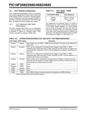
Capture/ and Compare operations described in this
chapter apply to all standard and Enhanced CCP1
modules. The operations of PWM mode, described in
Section 15.4 “PWM Mode”, apply to CCP1 only.
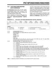
REGISTER 15-1: CCP1CON: CAPTURE/COMPARE/PWM CONTROL REGISTER
U-0 U-0 R/W-0 R/W-0 R/W-0 R/W-0 R/W-0 R/W-0
— — DC1B1 DC1B0 CCP1M3 CCP1M2 CCP1M1 CCP1M0
bit 7 bit 0
Legend:
R = Readable bit W = Writable bit U = Unimplemented bit, read as ‘0’
-n = Value at POR ‘1’ = Bit is set ‘0’ = Bit is cleared x = Bit is unknown
bit 7-6 Unimplemented: Read as ‘0’
bit 5-4 DC1B1:DC1B0: CCP1 Module PWM Duty Cycle bit 1 and bit 0
Capture mode:
Unused.
Compare mode:
Unused.
PWM mode:
These bits are the two LSbs (bit 1 and bit 0) of the 10-bit PWM duty cycle. The eight MSbs
(DC1B9:DC1B2) of the duty cycle are found in CCPR1L.
bit 3-0 CCP1M3:CCP1M0: CCP1 Module Mode Select bits
0000 = Capture/Compare/PWM disabled (resets CCP1 module)
0001 = Reserved
0010 = Compare mode; toggle output on match (CCP1IF bit is set)
0011 = Reserved
0100 = Capture mode; every falling edge or CAN message received (time-stamp)
(1)
0101 = Capture mode; every rising edge or CAN message received (time-stamp)
(1)
0110 = Capture mode; every 4th rising edge or every 4th CAN message received (time-stamp)
(1)
0111 = Capture mode; every 16th rising edge or every 16th CAN message received (time-stamp)
(1)
1000 = Compare mode; initialize CCP1 pin low; on compare match, force CCP1 pin high
(CCPIF bit is set)
1001 = Compare mode; initialize CCP pin high; on compare match, force CCP1 pin low
(CCPIF bit is set)
1010 = Compare mode; generate software interrupt on compare match (CCP1IF bit is set,
CCP1 pin reflects I/O state)
1011 = Compare mode; trigger special event; reset timer (TMR1 or TMR3, CCP1IF bit is set)
11xx =PWM mode
Note 1: Selected by CANCAP (CIOCON<4>) bit; overrides the CCP1 input pin source.
器件 Datasheet 文档搜索
AiEMA 数据库涵盖高达 72,405,303 个元件的数据手册,每天更新 5,000 多个 PDF 文件
