Datasheet 搜索 > 接口芯片 > NXP(恩智浦) > SGTL5000XNAA3 数据手册 > SGTL5000XNAA3 数据手册 4/68 页
 器件3D模型
¥ 19.932
SGTL5000XNAA3 数据手册 - NXP(恩智浦)
制造商:
NXP(恩智浦)
分类:
接口芯片
封装:
QFN-32
描述:
NXP SGTL5000XNAA3 音频编解码器, 耳机, 立体声, 1, 1, -40 °C, 85 °C, 96 kSPS
Pictures:
3D模型
符号图
焊盘图
引脚图
产品图
页面导航:
引脚图在P3P4Hot
典型应用电路图在P13P15P59P60
原理图在P2P12P20P23P59P60
封装尺寸在P61P62P63P64P65P66
型号编码规则在P1
封装信息在P61P62P63P64P65P66
功能描述在P3P12P13P14P15P16
技术参数、封装参数在P1P9
应用领域在P13P15P59P60
电气规格在P5P6P7P8P9P10P11P13
导航目录
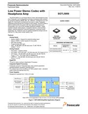
SGTL5000XNAA3数据手册
Page:
of 68 Go
若手册格式错乱,请下载阅览PDF原文件
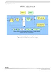
Analog Integrated Circuit Device Data
4 Freescale Semiconductor
SGTL5000
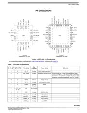
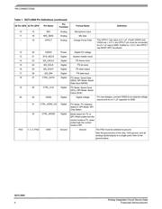
PIN CONNECTIONS
10 15 MIC Analog Microphone input
11 16 MIC_BIAS Analog Mic bias
— 18 CPFILT Analog Charge Pump Filter
The CPFILT cap value is 0.1 F. If both VDDIO and
VDDA are 3.0
V, the CPFILT pin must be connected
to a 0.1
F cap to GND. If either is > 3.0 V, the CPFILT
cap MUST NOT be placed.
12 20 VDDIO Power Digital I/O voltage
13 21 SYS_MCLK Digital System master clock
14 23 I2S_LRCLK Digital I
2
S frame clock
15 24 I2S_SCLK Digital I
2
S bit clock
16 25 I2S_DOUT Digital I
2
S data output
17 26 I2S_DIN Digital I
2
S data input
18 27 CTRL_DATA Digital
I
2
C Mode: Serial Data
(SDA); SPI Mode: Serial
Data Input (MOSI)
19 29 CTRL_CLK Digital
I
2
C Mode: Serial Clock
(SCL); SPI Mode: Serial
Clock (SCK)
20 30 VDDD Digital Digital voltage
For new designs, connect VDDD to an external voltage
source and to a 0.1
F capacitor to GND.
- 31 CTRL_ADR0_CS Digital
I
2
C Mode: I
2
C Address
Select 0; SPI Mode: SPI
Chip Select
- 32 CTRL_MODE Digital
Mode select for I
2
C or
SPI; When pulled low the
control mode is I
2
C, when
pulled high the control
mode is SPI
PAD 1, 3, 4, PAD GND Ground Ground The PAD must be soldered to ground.
Star the ground pins of the chip, VAG ground, and all
analog inputs/outputs to a single point, then to the
ground plane.
Table 1. SGTL5000 Pin Definitions (continued)
20 Pin QFN 32 Pin QFN Pin Name
Pin
Function
Formal Name Definition
器件 Datasheet 文档搜索
AiEMA 数据库涵盖高达 72,405,303 个元件的数据手册,每天更新 5,000 多个 PDF 文件
