Datasheet 搜索 > 接口芯片 > NXP(恩智浦) > SGTL5000XNAA3 数据手册 > SGTL5000XNAA3 数据手册 59/68 页
 器件3D模型
¥ 19.932
SGTL5000XNAA3 数据手册 - NXP(恩智浦)
制造商:
NXP(恩智浦)
分类:
接口芯片
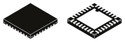
封装:
QFN-32
描述:
NXP SGTL5000XNAA3 音频编解码器, 耳机, 立体声, 1, 1, -40 °C, 85 °C, 96 kSPS
Pictures:
3D模型
符号图
焊盘图
引脚图
产品图
页面导航:
引脚图在P3P4Hot
典型应用电路图在P13P15P59P60
原理图在P2P12P20P23P59P60
封装尺寸在P61P62P63P64P65P66
型号编码规则在P1
封装信息在P61P62P63P64P65P66
功能描述在P3P12P13P14P15P16
技术参数、封装参数在P1P9
应用领域在P13P15P59P60
电气规格在P5P6P7P8P9P10P11P13
导航目录
SGTL5000XNAA3数据手册
Page:
of 68 Go
若手册格式错乱,请下载阅览PDF原文件
Analog Integrated Circuit Device Data
Freescale Semiconductor 59
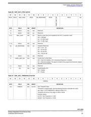
SGTL5000
TYPICAL APPLICATIONS
INTRODUCTION
TYPICAL APPLICATIONS
INTRODUCTION
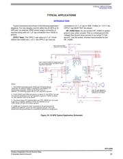
Typical connections are shown in the following application
diagrams. For new designs, and for either the 20 QFN or 32
QFN part, an external VDDD power supply connection is
required along with a 0.1
F cap connection from VDDD to
ground.
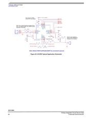
CPFILT Note: The CPFILT cap value is 0.1 F. If both
VDDIO and VDDA are 3.0
V, the CPFILT pin must be
connected to a 0.1
F cap to GND. If either is > 3.0 V, the
CPFILT cap MUST NOT be placed.
HP_VGND Note: Do not connect HP_VGND to system
ground, even when unused. This is a virtual ground (DC
voltage) that should never connect to an actual “0
Volt
ground”. Use the widest, shortest trace possible for the
HP_VGND.
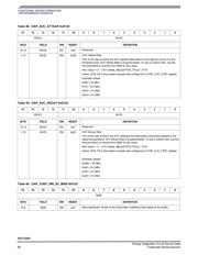
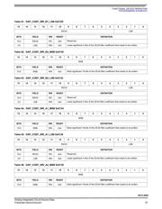
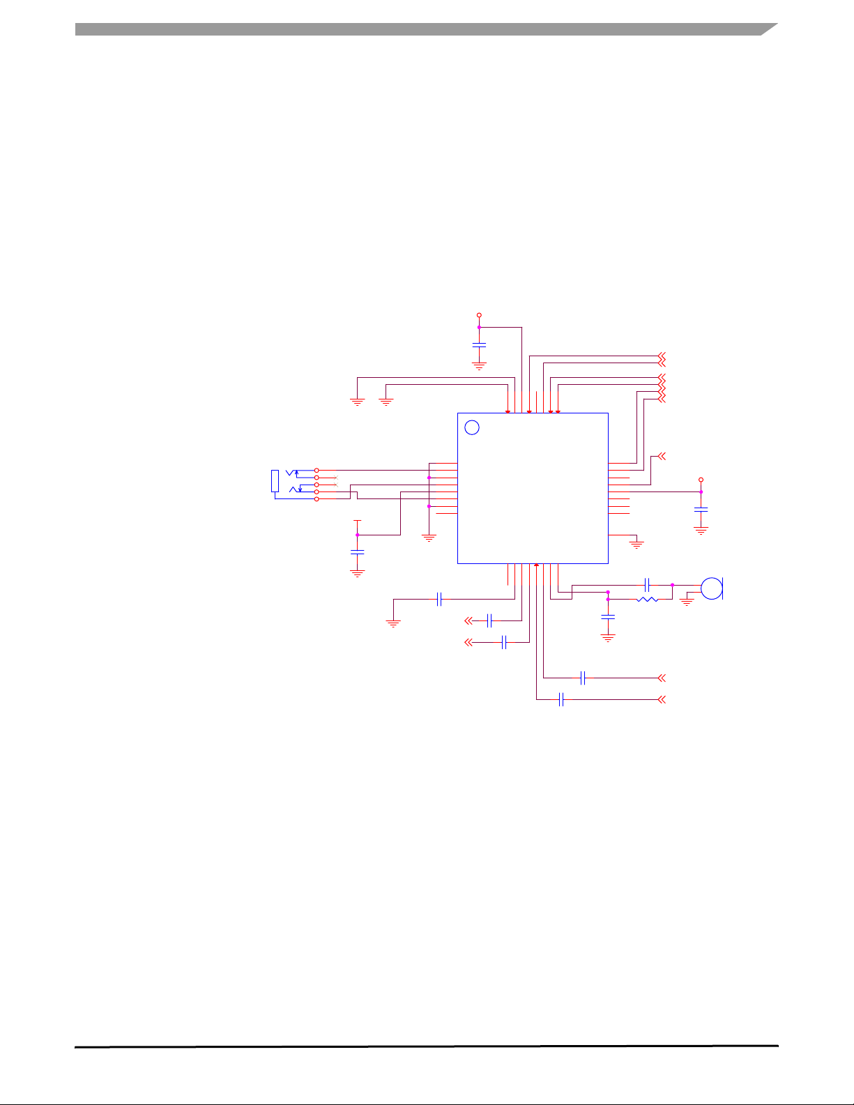
Figure 19. 32 QFN Typical Application Schematic
Notes:
1. This 32QFN schematic shows VDDD (pin 30) being derived
externally. An external VDDD is required for new designs. For
lowest power operation, VDDD can be driven from an
external 1.2V switching supply with a 0.1uF capacitor to ground.
2. If both VDDIO and VDDA are equal to or below 3V, the CPFILT pin (pin
17) must be connected to a 0.1uF capacitor to ground. If either is above
3V, this capacitor must not be placed.
3. The above shows I2C implementation as CTRL_MODE (pin 32) is tied
to ground. In addition, address 0 of the I2C address is 0 as
CTRL_ADR0_CS (pin 31) is tied to ground.
4. AGND (pin 7) should be "star" connected to the jack grounds for
LINEIN and LINEOUT, and to the VAG capacitor ground. This node
should via to the ground plane (or connected to ground) at a single point.
32QFN Typical Application Schematic
Solder Pad to GND
Note: R1 only needed if
internal BIAS_RESISTOR
settings are not suitable.
Note: External VDDD
required for new designs.
Note: Capless headphone design shown here.
For cap-coupled design, see 20QFN Typical
Application Schematic.
VDDIO
VDDA
VDDD (1.1V - 2.0V, 11mA Min)
CTRL_CLK
I2S_SCLK
CTRL_DATA
I2S_DIN
I2S_DOUT
SYS_MCLK
I2S_LRCLK
LINE_IN_L
LINE_IN_R
LINE_OUT_R
LINE_OUT_L
C1
0.1uF
C4 0.1uF
C3
0.1uF
U1
SGTL5000_32QFN
I2S_SCLK
24
NC
22
LINEIN_L
14
CPFILT
18
VDDIO
20
NC
19
SYS_MCLK
21
I2S_DOUT
25
I2S_DIN
26
HP_L
6
CTRL_DATA
27
NC
28
CTRL_CLK
29
GND
1
NC
8
HP_R
2
GND
3
VDDA
5
LINEOUT_L
12
LINEOUT_R
11
MIC
15
NC
17
LINEIN_R
13
AGND
7
I2S_LRCLK
23
VDDD
30
CTRL_ADR0_CS
31
CTRL_MODE
32
HP_VGND
4
NC
9
VAG
10
MIC_BIAS
16
GND
PAD
C10 1uF
C7
1uF
X1
MIC
1
2
J1
Audio Jack
2
5
1
4
3
C5 0.1uF
C6 1uF
C8 1uF
C9 1uF
C2
0.1uF
R1 2.2k
器件 Datasheet 文档搜索
AiEMA 数据库涵盖高达 72,405,303 个元件的数据手册,每天更新 5,000 多个 PDF 文件
