Datasheet 搜索 > 接口芯片 > TI(德州仪器) > SN65LVDS2DBVT 数据手册 > SN65LVDS2DBVT 数据手册 1/42 页

¥ 12.988
SN65LVDS2DBVT 数据手册 - TI(德州仪器)
制造商:
TI(德州仪器)
分类:
接口芯片
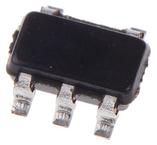
封装:
SOT-23-5
描述:
TEXAS INSTRUMENTS SN65LVDS2DBVT 差分线形驱动器, 1 驱动器
Pictures:
3D模型
符号图
焊盘图
引脚图
产品图
页面导航:
引脚图在P3P4Hot
典型应用电路图在P19
原理图在P1P14P15P16P17
封装尺寸在P33P34P36P37
标记信息在P33P34
封装信息在P32P33P34P35P36P37
技术参数、封装参数在P4
应用领域在P1P19P42
电气规格在P5P6P20
导航目录
SN65LVDS2DBVT数据手册
Page:
of 42 Go
若手册格式错乱,请下载阅览PDF原文件
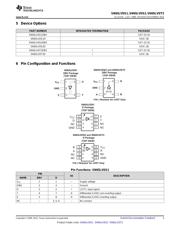
V
CC
GND
LVTTL
Out
V
CC
GND
D
NC
Z
NC
Y
NC
V
SUPPLY
100 TraceW
SN65LVDS1
B
NC
A
NC
V
CC
GND
R
NC
SN65LVDT2
V
CC
V
CC
GND
LVTTL
In
Product
Folder
Sample &
Buy
Technical
Documents
Tools &
Software
Support &
Community
SN65LVDS1
,
SN65LVDS2
,
SN65LVDT2
SLLS373L –JULY 1999–REVISED DECEMBER 2014
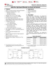
SN65LVDxx High-Speed Differential Line Drivers and Receivers
1 Features 2 Applications
1
• Meets or Exceeds the ANSI TIA/EIA-644 Standard
• Wireless Infrastructure
• Designed for Signaling Rates
(1)
up to: • Telecom Infrastructure
• Printer
– 630 Mbps for Drivers
– 400 Mbps for Receivers
3 Description
• Operates From a 2.4-V to 3.6-V Supply
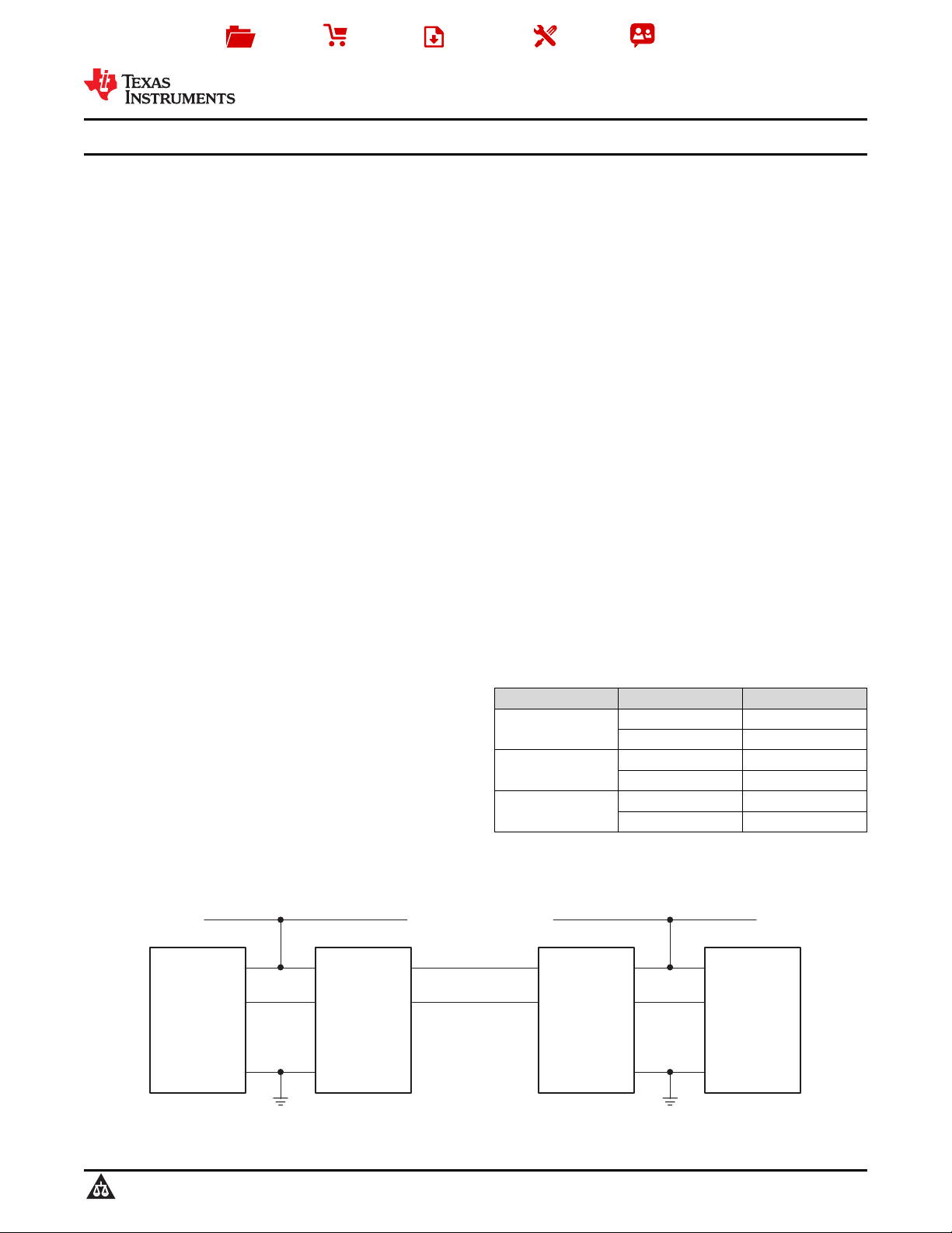
The SN65LVDS1, SN65LVDS2, and SN65LVDT2
• Available in SOT-23 and SOIC Packages
devices are single, low-voltage, differential line
• Bus-Terminal ESD Exceeds 9 kV
drivers and receivers in the small-outline transistor
package. The outputs comply with the TIA/EIA-644
• Low-Voltage Differential Signaling With Typical
standard and provide a minimum differential output
Output Voltages of 350 mV Into a 100-Ω Load
voltage magnitude of 247 mV into a 100-Ω load at
• Propagation Delay Times
signaling rates up to 630 Mbps for drivers and 400
– 1.7-ns Typical Driver
Mbps for receivers.
– 2.5-ns Typical Receiver
When the SN65LVDS1 device is used with an LVDS
• Power Dissipation at 200 MHz
receiver (such as the SN65LVDT2) in a point-to-point
connection, data or clocking signals can be
– 25 mW Typical Driver
transmitted over printed-circuit board traces or cables
– 60 mW Typical Receiver
at very high rates with very low electromagnetic
• LVDT Receiver Includes Line Termination
emissions and power consumption. The packaging,
low power, low EMI, high ESD tolerance, and wide
• Low Voltage TTL (LVTTL) Level Driver Input Is 5-
supply voltage range make the device ideal for
V Tolerant
battery-powered applications.
• Driver Is Output High-Impedance with
The SN65LVDS1, SN65LVDS2, and SN65LVDT2
V
CC
< 1.5 V
devices are characterized for operation from –40°C to
• Receiver Output and Inputs are High-Impedance
85°C.
With V
CC
< 1.5 V
• Receiver Open-Circuit Fail Safe
Device Information
(1)
• Differential Input Voltage Threshold Less Than
PART NUMBER PACKAGE BODY SIZE (NOM)
100 mV
SOIC (8) 4.90 mm × 3.91 mm
SN65LVDS1
SOT (5) 2.90 mm × 1.60 mm
SOIC (8) 4.90 mm × 3.91 mm
SN65LVDS2
SOT (5) 2.90 mm × 1.60 mm
SOIC (8) 4.90 mm × 3.91 mm
SN65LVDT2
SOT (5) 2.90 mm × 1.60 mm
(1) The signaling rate of a line is the number of voltage
(1) For all available packages, see the orderable addendum at
transitions that are made per second expressed in the units
the end of the data sheet.
bps (bit per second)
Simplified Schematic
1
An IMPORTANT NOTICE at the end of this data sheet addresses availability, warranty, changes, use in safety-critical applications,
intellectual property matters and other important disclaimers. PRODUCTION DATA.
器件 Datasheet 文档搜索
AiEMA 数据库涵盖高达 72,405,303 个元件的数据手册,每天更新 5,000 多个 PDF 文件
