Datasheet 搜索 > 接口芯片 > TI(德州仪器) > SN65LVDS2DBVT 数据手册 > SN65LVDS2DBVT 数据手册 4/42 页

¥ 12.988
SN65LVDS2DBVT 数据手册 - TI(德州仪器)
制造商:
TI(德州仪器)
分类:
接口芯片
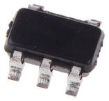
封装:
SOT-23-5
描述:
TEXAS INSTRUMENTS SN65LVDS2DBVT 差分线形驱动器, 1 驱动器
Pictures:
3D模型
符号图
焊盘图
引脚图
产品图
页面导航:
引脚图在P3P4Hot
典型应用电路图在P19
原理图在P1P14P15P16P17
封装尺寸在P33P34P36P37
标记信息在P33P34
封装信息在P32P33P34P35P36P37
技术参数、封装参数在P4
应用领域在P1P19P42
电气规格在P5P6P20
导航目录
SN65LVDS2DBVT数据手册
Page:
of 42 Go
若手册格式错乱,请下载阅览PDF原文件
SN65LVDS1
,
SN65LVDS2
,
SN65LVDT2
SLLS373L –JULY 1999–REVISED DECEMBER 2014
www.ti.com
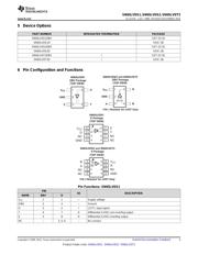
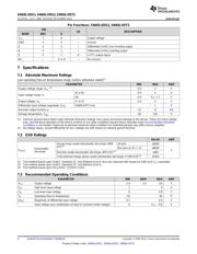
Pin Functions: SN65LVDS2, SN65LVDT2
PIN
I/O DESCRIPTION
NAME DBV D
V
CC
1 8 -- Supply voltage
GND 2 5 -- Ground
A 3 2 I Differential (LVDS) non-inverting output
B 4 1 I Differential (LVDS) inverting output
R 5 7 O LVTTL output signal
NC -- 3, 4, 6 -- No connect
7 Specifications
7.1 Absolute Maximum Ratings
over operating free-air temperature range (unless otherwise noted)
(1)
PARAMETER MIN MAX UNIT
Supply voltage range, V
CC
(2)
–0.5 4 V
(A or B) –0.5 4 V
Input voltage range, V
I
(D) –0.5 V
CC
+ 2 V
Output voltage, V
O
(Y or Z) –0.5 4 V
Differential input voltage magnitude, |V
ID
| SN65LVDT2 only 1 V
Receiver output current, I
O
–12 12 mA
Storage temperature, T
stg
–65 150 °C
(1) Stresses beyond those listed under Absolute Maximum Ratings may cause permanent damage to the device. These are stress ratings
only, and functional operation of the device at these or any other conditions beyond those indicated under Recommended Operating
Conditions is not implied. Exposure to absolute-maximum-rated conditions for extended periods may affect device reliability.
(2) All voltage values, except differential I/O bus voltages are with respect to network ground terminal.
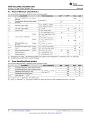
7.2 ESD Ratings
VALUE UNIT
Human-body model electrostatic discharge, HBM All pins ±4000
ESD
(1)
Bus pins (A, B, Y, Z) ±9000
Electrostatic
V
(ESD)
V
discharge
Machine-model electrostatic discharge, MM ESD
(2)
±400
Field-induced-charge device model electrostatic discharge, FCDM ESD
(3)
±1500
(1) Test method based upon JEDEC Standard 22, Test Method A114-A. Bus pins stressed with respect to GND and V
CC
separately.
(2) Test method based upon JEDEC Standard 22, Test Method A114-A.
(3) Test method based upon EIA-JEDEC JESD22-C101C.
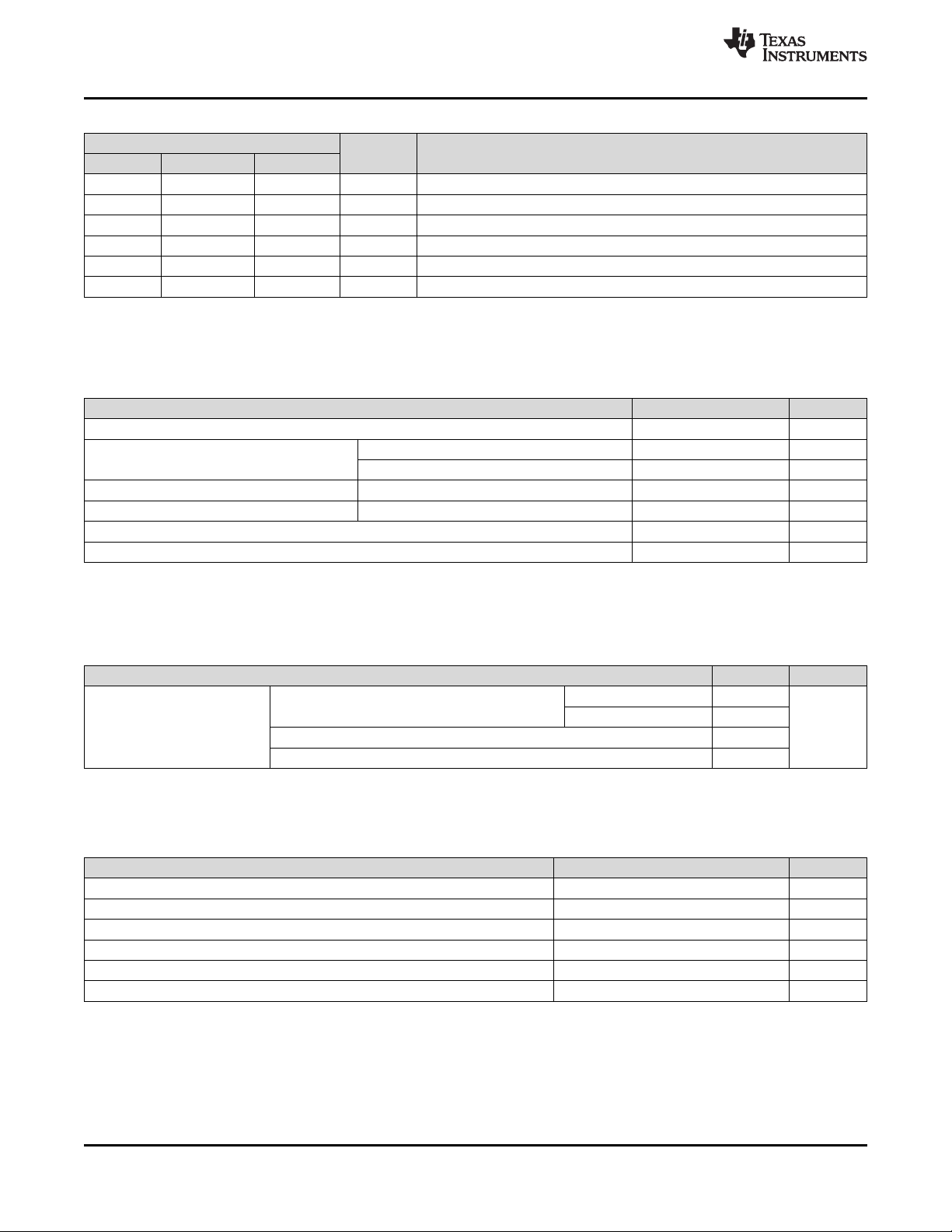
7.3 Recommended Operating Conditions
PARAMETER MIN NOM MAX UNIT
V
CC
Supply voltage 2.4 3.3 3.6 V
V
IH
High-level input voltage 2 5 V
V
IL
Low-level input voltage 0 0.8 V
T
A
Operating free-air temperature –40 85 °C
|V
ID
| Magnitude of differential input voltage 0.1 0.6 V
Input voltage (any combination of input or common-mode voltage) 0 V
CC
– 0.8 V
4 Submit Documentation Feedback Copyright © 1999–2014, Texas Instruments Incorporated
Product Folder Links: SN65LVDS1 SN65LVDS2 SN65LVDT2
器件 Datasheet 文档搜索
AiEMA 数据库涵盖高达 72,405,303 个元件的数据手册,每天更新 5,000 多个 PDF 文件
