Datasheet 搜索 > 接口芯片 > TI(德州仪器) > SN65LVDS2DBVT 数据手册 > SN65LVDS2DBVT 数据手册 6/42 页

¥ 12.988
SN65LVDS2DBVT 数据手册 - TI(德州仪器)
制造商:
TI(德州仪器)
分类:
接口芯片
封装:
SOT-23-5
描述:
TEXAS INSTRUMENTS SN65LVDS2DBVT 差分线形驱动器, 1 驱动器
Pictures:
3D模型
符号图
焊盘图
引脚图
产品图
页面导航:
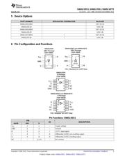
引脚图在P3P4Hot
典型应用电路图在P19
原理图在P1P14P15P16P17
封装尺寸在P33P34P36P37
标记信息在P33P34
封装信息在P32P33P34P35P36P37
技术参数、封装参数在P4
应用领域在P1P19P42
电气规格在P5P6P20
导航目录
SN65LVDS2DBVT数据手册
Page:
of 42 Go
若手册格式错乱,请下载阅览PDF原文件
SN65LVDS1
,
SN65LVDS2
,
SN65LVDT2
SLLS373L –JULY 1999–REVISED DECEMBER 2014
www.ti.com
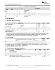
7.6 Receiver Electrical Characteristics
over recommended operating conditions (unless otherwise noted)
PARAMETER TEST CONDITIONS MIN
(1)
TYP
(2)
MAX UNIT
Positive-going differential input voltage
V
ITH+
100
threshold
See Figure 11 mV
Negative-going differential input voltage
V
ITH–
–100
threshold
I
OH
= –8 mA, V
CC
= 2.4 V 1.9
V
OH
High-level output voltage V
I
OH
= –8 mA, V
CC
= 3 V 2.4
V
OL
Low-level output voltage I
OL
= 8 mA 0.25 0.4 V
I
CC
Supply current No load, Steady state 4 7 mA
V
I
= 0 V, other input = 1.2 V –20 –2
LVDS2
V
I
= 2.2 V, other input = 1.2 V,
–3 –1.2
V
CC
= 3.0 V
I
I
Input current (A or B inputs) μA
V
I
= 0 V, other input open –40 -4
LVDT2
V
I
= 2.2 V, other input open,
–6 –2.4
V
CC
= 3.0 V
Differential input current
I
ID
LVDS2 V
IA
= 2.4 V, V
IB
= 2.3 V –2 2 μA
(I
IA
– I
IB
)
LVDS2 V
CC
= 0 V, V
IA
= V
IB
= 2.4 V 20
Power-off input current (A or B
I
I(OFF)
μA
inputs)
LVDT2 V
CC
= 0 V, V
IA
= V
IB
= 2.4 V 40
R
T
Differential input resistance LVDT2 V
IA
= 2.4 V, V
IB
= 2.2 V 90 111 132 Ω
C
I
Input capacitance V
I
= 0.4sin(4E6πt) + 0.5 V 5.8 pF
C
O
Output capacitance V
I
= 0.4sin(4E6πt) + 0.5 V 3.4 pF
(1) The algebraic convention, in which the least positive (most negative) limit is designated as a minimum, is used in this data sheet.
(2) All typical values are at 25°C and with a 2.7-V supply.
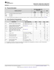
7.7 Driver Switching Characteristics
over recommended operating conditions (unless otherwise noted)
PARAMETER TEST CONDITIONS MIN TYP
(1)
MAX UNIT
t
PLH
Propagation delay time, low-to-high-level output 1.5 3.1 ns
t
PHL
Propagation delay time, high-to-low-level output 1.8 3.1 ns
R
L
= 100 Ω, C
L
= 10 pF,
t
r
Differential output signal rise time 0.6 1 ns
See Figure 13
t
f
Differential output signal fall time 0.7 1 ns
t
sk(p)
Pulse skew (|t
PHL
– t
PLH
|)
(2)
0.3 ns
(1) All typical values are at 25°C and with a 3.3-V supply.
(2) t
sk(p)
is the magnitude of the time difference between the high-to-low and low-to-high propagation delay times at an output.
6 Submit Documentation Feedback Copyright © 1999–2014, Texas Instruments Incorporated
Product Folder Links: SN65LVDS1 SN65LVDS2 SN65LVDT2
器件 Datasheet 文档搜索
AiEMA 数据库涵盖高达 72,405,303 个元件的数据手册,每天更新 5,000 多个 PDF 文件
