Datasheet 搜索 > 接口芯片 > TI(德州仪器) > SN65LVDS2DBVT 数据手册 > SN65LVDS2DBVT 数据手册 15/42 页

¥ 12.988
SN65LVDS2DBVT 数据手册 - TI(德州仪器)
制造商:
TI(德州仪器)
分类:
接口芯片
封装:
SOT-23-5
描述:
TEXAS INSTRUMENTS SN65LVDS2DBVT 差分线形驱动器, 1 驱动器
Pictures:
3D模型
符号图
焊盘图
引脚图
产品图
页面导航:
引脚图在P3P4Hot
典型应用电路图在P19
原理图在P1P14P15P16P17
封装尺寸在P33P34P36P37
标记信息在P33P34
封装信息在P32P33P34P35P36P37
技术参数、封装参数在P4
应用领域在P1P19P42
电气规格在P5P6P20
导航目录
SN65LVDS2DBVT数据手册
Page:
of 42 Go
若手册格式错乱,请下载阅览PDF原文件
V
CC
50 W
300kW
7V
DInput
V
CC
7V
10kW
5 W
Y orZOutput
S0313-02
SN65LVDS1
,
SN65LVDS2
,
SN65LVDT2
www.ti.com
SLLS373L –JULY 1999–REVISED DECEMBER 2014
Feature Description (continued)
9.3.1.3 5-V Input Tolerance
5-V and 3.3-V TTL logic standards share the same input high-voltage and input low-voltage thresholds, namely
2.0 V and 0.8 V, respectively. Although the maximum supply voltage for the SN65LVDS1 is 3.6 V, the driver can
operate and meet all performance requirements when the input signals are as high as 5 V. This allows operation
with 3.3-V TTL as well as 5-V TTL logic. 3.3-V CMOS and 5-V CMOS inputs are also allowable, although one
should ensure that the duty-cycle distortion that will result from the TTL (ground-referenced) thresholds are
acceptable.
9.3.1.4 NC Pins
NC (not connected) pins are pins where the die is not physically connected to the lead frame or package. For
optimum thermal performance, a good rule of thumb is to ground the NC pins at the board level.
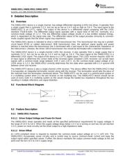
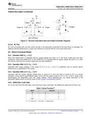
9.3.1.5 Driver Equivalent Schematics
The SN65LVDS1 equivalent input and output schematic diagrams are shown in Figure 15. The driver input is
represented by a CMOS inverter stage with a 7-V Zener diode. The input stage is high-impedance, and includes
an internal pulldown to ground. If the driver input is left open, the driver input provides a low-level signal to the
rest of the driver circuitry, resulting in a low-level signal at the driver output pins. The Zener diode provides ESD
protection. The driver output stage is a differential pair, one half of which is shown in Figure 15. Like the input
stage, the driver output includes a Zener diode for ESD protection. The schematic shows an output stage that
includes a set of current sources (nominally 3.5 mA) that are connected to the output load circuit based upon the
input stage signal. To the first order, the SN65LVDS2 output stage acts a constant-current source.
Figure 15. Driver Equivalent Input and Output Schematic Diagrams
9.3.2 SN65LVDS2 and SN65LVDT2 Features
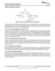
9.3.2.1 Receiver Open Circuit Fail-Safe
One of the most common problems with differential signaling applications is how the system responds when no
differential voltage is present on the signal pair. The LVDS receiver is like most differential line receivers in that
its output logic state can be indeterminate when the differential input voltage is between –100 mV and 100 mV
and within its recommended input common-mode voltage range. However, the TI LVDS receiver is different in
how it handles the open-input circuit situation.
Open circuit means that there is little or no input current to the receiver from the data line itself. This could be
when the driver is in a high-impedance state or the cable is disconnected. When this occurs, the LVDS receiver
pulls each line of the signal to V
CC
through 300-kΩ resistors as shown in Figure 16. The fail-safe feature uses an
AND gate with input voltage thresholds at about 2.3 V to detect this condition and force the output to a high level.
Copyright © 1999–2014, Texas Instruments Incorporated Submit Documentation Feedback 15
Product Folder Links: SN65LVDS1 SN65LVDS2 SN65LVDT2
器件 Datasheet 文档搜索
AiEMA 数据库涵盖高达 72,405,303 个元件的数据手册,每天更新 5,000 多个 PDF 文件
