Datasheet 搜索 > 接口芯片 > TI(德州仪器) > SN65LVDS2DBVT 数据手册 > SN65LVDS2DBVT 数据手册 16/42 页

¥ 12.988
SN65LVDS2DBVT 数据手册 - TI(德州仪器)
制造商:
TI(德州仪器)
分类:
接口芯片
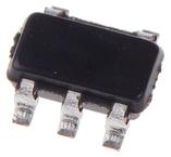
封装:
SOT-23-5
描述:
TEXAS INSTRUMENTS SN65LVDS2DBVT 差分线形驱动器, 1 驱动器
Pictures:
3D模型
符号图
焊盘图
引脚图
产品图
页面导航:
引脚图在P3P4Hot
典型应用电路图在P19
原理图在P1P14P15P16P17
封装尺寸在P33P34P36P37
标记信息在P33P34
封装信息在P32P33P34P35P36P37
技术参数、封装参数在P4
应用领域在P1P19P42
电气规格在P5P6P20
导航目录
SN65LVDS2DBVT数据手册
Page:
of 42 Go
若手册格式错乱,请下载阅览PDF原文件
Rt = 100 Ω (Typ)
300 kΩ 300 kΩ
V
CC
V
IT
≈ 2.3 V
A
B
Y
SN65LVDS1
,
SN65LVDS2
,
SN65LVDT2
SLLS373L –JULY 1999–REVISED DECEMBER 2014
www.ti.com
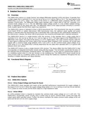
Feature Description (continued)
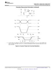
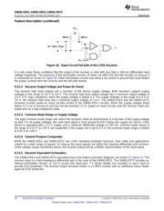
Figure 16. Open-Circuit Fail-Safe of the LVDS Receiver
It is only under these conditions that the output of the receiver is valid with less than a 100-mV differential input
voltage magnitude. The presence of the termination resistor, Rt does not affect the fail-safe function as long as it
is connected as shown in Figure 16. Other termination circuits may allow a dc-current to ground that could defeat
the pullup currents from the receiver and the fail-safe feature.
9.3.2.2 Receiver Output Voltage and Power-On Reset
The receiver high level outputs are a function of the device supply voltage. Both receivers support supply
voltages in the range of 2.6 V to 3.6 V. The receiver high level output voltage has a minimum output voltage of
2.4 V (TTL logic compliant), when the supply voltage is above 3 V. For supply voltages in the range of 2.6 V to
3.0 V, the receiver high level has a minimum output voltage of 1.9 V. The SN65LVDS2 and the SN65LVDT2
receivers include power-on reset circuitry similar to the SN65LVDS1 circuitry. When the supply voltage drops
below 1.5 V (or is turning on and has not yet reached 1.5 V), power-on reset circuitry sets the receiver input and
output pins to a high-impedance state.
9.3.2.3 Common-Mode Range vs Supply Voltage
The input common-mode range over which the receivers meet all requirements is a function of the supply voltage
as well. For all supply voltages, the valid input signal is from ground to 0.8 V below the supply rail. Hence, if the
device is operating with a 3.3 V supply, and a minimum differential voltage of 100 mV, common-mode values in
the range of 0.05 V to 2.45 V are supported. If the supply rail is set to 2.5 V, the common-mode range is limited
to 0.05 V to 1.65 V.
9.3.2.4 General Purpose Comparator
While the SN65LVDS2 and SN65LVDT2 are LVDS standard-compliant receivers, their utility and applications
extend to a wider range of signals. As long as the input signals are within the required differential and common-
mode voltage ranges mentioned above, the receiver output will be a faithful representation of the input signal.
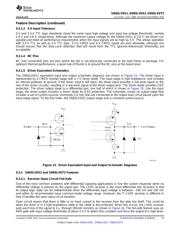
9.3.2.5 Receiver Equivalent Schematics
The SN65LVDS2 and SN65LVDT2 equivalent input and output schematic diagrams are shown in Figure 17. The
receiver input is a high-impedance differential pair in the case of the SN65LVDS2. The SN65LVDT2 includes an
internal termination resistor of 110 Ω across the input port. 7-V Zener diodes are included on each input to
provide ESD protection. The receiver output structure shown is a CMOS inverter with an additional Zener diode,
again for ESD protection.
16 Submit Documentation Feedback Copyright © 1999–2014, Texas Instruments Incorporated
Product Folder Links: SN65LVDS1 SN65LVDS2 SN65LVDT2
器件 Datasheet 文档搜索
AiEMA 数据库涵盖高达 72,405,303 个元件的数据手册,每天更新 5,000 多个 PDF 文件
